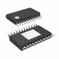
LTC3862HFE#PBF Linear Technology, LTC3862HFE#PBF Datasheet - Page 34

LTC3862HFE#PBF
Manufacturer Part Number
LTC3862HFE#PBF
Description
IC CTRLR DC/DC MULTI-PH 24TSSOP
Manufacturer
Linear Technology
Type
Step-Up (Boost)r
Datasheet
1.LTC3862EGNPBF.pdf
(40 pages)
Specifications of LTC3862HFE#PBF
Internal Switch(s)
No
Synchronous Rectifier
No
Number Of Outputs
1
Voltage - Output
1.22 ~ 200 V
Current - Output
50mA
Frequency - Switching
300kHz
Voltage - Input
4 ~ 36 V
Operating Temperature
-40°C ~ 150°C
Mounting Type
Surface Mount
Package / Case
24-TSSOP Exposed Pad, 24-eTSSOP, 24-HTSSOP
Lead Free Status / RoHS Status
Lead free / RoHS Compliant
Power - Output
-
LTC3862
APPLICATIONS INFORMATION
PC Board Layout Checklist
When laying out the printed circuit board, the following
checklist should be used to ensure proper operation of
the converter:
1. For lower power applications a 2-layer PC board is suf-
34
Figure 26. LTC3862 Switching Waveforms for Boost Converter
AC COUPLED
100mV/DIV
For the bulk capacitance, which we assume contributes
1% to the total output ripple, the minimum required
capacitance is approximately:
For this application, in order to obtain both low ESR
and an adequate ripple current rating (see Figure 23),
two 100μF , 63V aluminum electrolytic capacitors were
connected in parallel with four 6.8μF , 50V ceramic
capacitors. Figure 26 illustrates the switching wave-
forms for this application circuit.
fi cient. However, for higher power levels, a multilayer
PC board is recommended. Using a solid ground plane
and proper component placement under the circuit is
the easiest way to ensure that switching noise does
not affect the operation.
C
50V/DIV
50V/DIV
OUT
5A/DIV
5A/DIV
V
SW1
SW2
OUT
I
I
L2
L1
≥
= 17 5 .
V
V
IN
OUT
0 01
= 24V
.
= 48V, 1.5A
μF
I
• •
O MAX
n V
(
OUT
)
2.5μs/DIV
•
f
=
0 01 2 48
.
• •
3862 F26
5
A
V
•
300 H H z
k
T
2. In order to help dissipate the power from the MOSFETs
3. Place all power components in a tight area. This will
4. Orient the input and output capacitors and current
5. Place the INTV
6. Use a local via to ground plane for all pads that
7. Place the small-signal components away from high
8. The exposed area on the bottom of the QFN package
9. The MOSFETs should also be placed on the same
and diodes, keep the ground plane on the layers closest
to the power components. Use power planes for the
MOSFETs and diodes in order to maximize the heat
spreading from these components into the PCB.
minimize the size of high current loops. The high di/dt
loops formed by the sense resistor, power MOSFET,
the boost diode and the output capacitor should be
kept as small as possible to avoid EMI.
sense resistors in a way that minimizes the distance
between the pads connected to the ground plane.
Keep the capacitors for INTV
as possible to LTC3862.
possible to the INTV
layer as the IC. A low ESR (X5R or better) 4.7μF to
10μF ceramic capacitor should be used.
connect to the ground. Use multiple vias for power
components.
frequency switching nodes on the board. The pinout
of the LTC3862 was carefully designed in order to
make component placement easy. All of the power
components can be placed on one side of the IC, away
from all of the small-signal components.
is internally connected to PGND; however it should
not be used as the main path for high current fl ow.
layer of the board as the sense resistors. The MOSFET
source should connect to the sense resistor using a
short, wide PCB trace.
CC
decoupling capacitor as close as
CC
and PGND pins, on the same
CC
, 3V8 and V
IN
as close
3862fb


