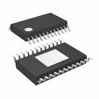
LTC3862HFE#PBF Linear Technology, LTC3862HFE#PBF Datasheet - Page 18

LTC3862HFE#PBF
Manufacturer Part Number
LTC3862HFE#PBF
Description
IC CTRLR DC/DC MULTI-PH 24TSSOP
Manufacturer
Linear Technology
Type
Step-Up (Boost)r
Datasheet
1.LTC3862EGNPBF.pdf
(40 pages)
Specifications of LTC3862HFE#PBF
Internal Switch(s)
No
Synchronous Rectifier
No
Number Of Outputs
1
Voltage - Output
1.22 ~ 200 V
Current - Output
50mA
Frequency - Switching
300kHz
Voltage - Input
4 ~ 36 V
Operating Temperature
-40°C ~ 150°C
Mounting Type
Surface Mount
Package / Case
24-TSSOP Exposed Pad, 24-eTSSOP, 24-HTSSOP
Lead Free Status / RoHS Status
Lead free / RoHS Compliant
Power - Output
-
LTC3862
Table 1
Using the LTC3862 Transconductance (g
Amplifi er in Multi-Phase Applications
The LTC3862 error amplifi er is a transconductance, or g
amplifi er, meaning that it has high DC gain but high output
impedance (the output of the error amplifi er is a current
proportional to the differential input voltage). This style
of error amplifi er greatly eases the task of implementing
a multi-phase solution, because the amplifi ers from two
or more chips can be connected in parallel. In this case
the FB pins of multiple LTC3862s can be connected to-
gether, as well as the ITH pins, as shown in Figure 8. The
g
transconductance of one amplifi er, or g
where n is the number of amplifi ers connected in paral-
lel. The transfer function from the ITH pin to the current
comparator inputs was carefully designed to be accurate,
both from channel-to-channel and chip-to-chip. This way
the peak inductor current matching is kept accurate.
A buffered version of the output of the error amplifi er
determines the threshold at the input of the current com-
parator. The ITH voltage that represents zero peak current
is 0.4V and the voltage that represents current limit is
1.2V (at low duty cycle). During an overload condition, the
output of the error amplifi er is clamped to 2.6V at low duty
cycle, in order to reduce the latency when the overload
condition terminates. A patented circuit in the LTC3862 is
used to recover the slope compensation signal, so that the
maximum peak inductor current is not a strong function
of the duty cycle.
Soft-Start
The start-up of the LTC3862 is controlled by the voltage on
the SS pin. An internal PNP transistor clamps the current
comparator sense threshold during soft-start, thereby
limiting the peak switch current. The base of the PNP is
connected to the SS pin and the emitter to an internal,
OPERATION
18
PHASEMODE
m
of the composite error amplifi er is simply n times the
SGND
Float
3V8
CH-1 to CH-2
PHASE
180°
180°
120°
CH-1 to CLKOUT
PHASE
240°
90°
60°
m(TOT)
m
2-Phase, 4-Phase
) Error
APPLICATION
= n • 660μS,
6-Phase
3-Phase
m
buffered ITH node (please note that the ITH pin voltage may
not track the soft-start voltage during this time period).
An internal 5μA current source charges the SS capacitor,
and clamps the peak sense threshold until the voltage on
the soft-start capacitor reaches approximately 0.6V. The
required amount of soft-start capacitance can be estimated
using the following equation:
The SS pin has an internal open-drain NMOS pull-down
transistor that turns on when the RUN pin is pulled low,
when the voltage on the INTV
lockout threshold, or during an overtemperature condi-
tion. In multi-phase applications that use more than one
ALL ITH PINS
CONNECTED
ALL FB PINS
CONNECTED
TOGETHER
TOGETHER
C
SS
V
OUT
Figure 8. LTC3862 Error Amplifi er Confi guration
for Multi-Phase Operation
=
5
μA
⎛
⎝ ⎜
0 6 .
t
SS
V
⎞
⎠ ⎟
FREQ
ITH
FB
CLKOUT
SYNC
PLLFLTR
FREQ
ITH
FB
CLKOUT
SYNC
PLLFLTR
FREQ
ITH
FB
CLKOUT
SYNC
PLLFLTR
CC
MASTER
LTC3862
LTC3862
LTC3862
SLAVE
SLAVE
SGND
SGND
SGND
pin is below its undervoltage
INTV
INTV
INTV
RUN
RUN
RUN
SS
SS
SS
CC
CC
CC
3862 F08
ALL RUN PINS
CONNNECTED
TOGETHER
ALL SS PINS
CONNNECTED
TOGETHER
ON/OFF
CONTROL
INDIVIDUAL
INTV
LOCALLY
DECOUPLED
CC
3862fb
PINS


