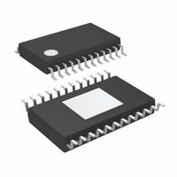
LTC3862HFE#PBF Linear Technology, LTC3862HFE#PBF Datasheet - Page 23

LTC3862HFE#PBF
Manufacturer Part Number
LTC3862HFE#PBF
Description
IC CTRLR DC/DC MULTI-PH 24TSSOP
Manufacturer
Linear Technology
Type
Step-Up (Boost)r
Datasheet
1.LTC3862EGNPBF.pdf
(40 pages)
Specifications of LTC3862HFE#PBF
Internal Switch(s)
No
Synchronous Rectifier
No
Number Of Outputs
1
Voltage - Output
1.22 ~ 200 V
Current - Output
50mA
Frequency - Switching
300kHz
Voltage - Input
4 ~ 36 V
Operating Temperature
-40°C ~ 150°C
Mounting Type
Surface Mount
Package / Case
24-TSSOP Exposed Pad, 24-eTSSOP, 24-HTSSOP
Lead Free Status / RoHS Status
Lead free / RoHS Compliant
Power - Output
-
The ITH series R
loop compensation. The transfer function for boost and
fl yback converters contains a right half plane zero that
normally requires the loop crossover frequency to be
reduced signifi cantly in order to maintain good phase
margin. The R
slightly (from 0.5 to 2 times their suggested values) to
optimize transient response once the fi nal PC layout is done
and the particular output capacitor type(s) and value(s)
have been determined. The output capacitor confi guration
needs to be selected in advance because the effective ESR
and bulk capacitance have a signifi cant effect on the loop
gain and phase. An output current pulse of 20% to 80%
of full-load current having a rise time of 1μs to 10μs will
produce output voltage and ITH pin waveforms that will
give a sense of the overall loop stability without breaking
the feedback loop. Placing a power MOSFET and load
resistor directly across the output capacitor and driving
OPERATION
C
• C
C
C
• C
fi lter values can typically be modifi ed
C
fi lter sets the dominant pole-zero
500mV/DIV
1A TO 5A
5A/DIV
5A/DIV
5A/DIV
I
V
LOAD
OUT
I
I
L1
L2
Figure 17. Load Step Response of a Properly
Compensated Boost Converter
V
V
IN
OUT
= 24V
= 48V
500μs/DIV
the gate with an appropriate signal generator is a practi-
cal way to produce a fast load step condition. The initial
output voltage step resulting from the step change in the
output current may not be within the bandwidth of the
feedback loop, so this signal cannot be used to determine
phase margin. This is why it is better to look at the ITH
pin signal which is in the feedback loop and is the fi ltered
and compensated control loop response. The gain of the
loop will be increased by increasing R
of the loop will be increased by decreasing C
increased by the same factor that C
zero frequency will be kept the same, thereby keeping the
phase shift the same in the most critical frequency range
of the feedback loop. The output voltage settling behavior
is related to the stability of the closed-loop system and
will demonstrate the actual overall supply performance.
Figure 17 illustrates the load step response of a properly
compensated boost converter.
3862 F17
C
C
and the bandwidth
is decreased, the
LTC3862
C
. If R
23
3862fb
C
is


