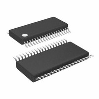
LTC3855IFE#PBF Linear Technology, LTC3855IFE#PBF Datasheet - Page 26

LTC3855IFE#PBF
Manufacturer Part Number
LTC3855IFE#PBF
Description
IC CTLR DC/DC MULTIPHASE 38SSOP
Manufacturer
Linear Technology
Series
PolyPhase®r
Type
Step-Down (Buck)r
Datasheet
1.LTC3855EUJPBF.pdf
(44 pages)
Specifications of LTC3855IFE#PBF
Internal Switch(s)
No
Synchronous Rectifier
Yes
Number Of Outputs
2
Voltage - Output
0.6 ~ 3.3 V, 0.6 ~ 12.5 V
Current - Output
25A
Frequency - Switching
250kHz ~ 770kHz
Voltage - Input
4.5 ~ 38 V
Operating Temperature
-40°C ~ 125°C
Mounting Type
Surface Mount
Package / Case
38-TSSOP Exposed Pad, 38-eTSSOP, 38-HTSSOP
Lead Free Status / RoHS Status
Lead free / RoHS Compliant
Power - Output
-
Available stocks
Company
Part Number
Manufacturer
Quantity
Price
LTC3855
applicaTions inForMaTion
can also be used for C
if there is any question.
The benefit of the LTC3855 2-phase operation can be cal-
culated by using the equation above for the higher power
controller and then calculating the loss that would have
resulted if both controller channels switched on at the same
time. The total RMS power lost is lower when both control-
lers are operating due to the reduced overlap of current
pulses required through the input capacitor’s ESR. This is
why the input capacitor’s requirement calculated above for
the worst-case controller is adequate for the dual controller
design. Also, the input protection fuse resistance, battery
resistance, and PC board trace resistance losses are also
reduced due to the reduced peak currents in a 2-phase
system. The overall benefit of a multiphase design will
only be fully realized when the source impedance of the
power supply/battery is included in the efficiency testing.
The sources of the top MOSFETs should be placed within
1cm of each other and share a common C
the sources and C
current resonances at V
A small (0.1µF to 1µF) bypass capacitor between the chip
V
suggested. A 2.2Ω to 10Ω resistor placed between C
(C1) and the V
the two channels.
The selection of C
resistance (ESR). Typically, once the ESR requirement
is satisfied, the capacitance is adequate for filtering. The
output ripple (∆V
where f is the operating frequency, C
capacitance and I
tor. The output ripple is highest at maximum input voltage
since I
Setting Output Voltage
The LTC3855 output voltages are each set by an external
feedback resistive divider carefully placed across the
IN
∆V
pin and ground, placed close to the LTC3855, is also
OUT
RIPPLE
≈I
RIPPLE
increases with input voltage.
IN
OUT
RIPPLE
IN
pin provides further isolation between
OUT
may produce undesirable voltage and
) is approximated by:
ESR +
IN
. Always consult the manufacturer
is driven by the effective series
IN
is the ripple current in the induc-
.
8fC
1
OUT
OUT
IN
(s). Separating
is the output
IN
output, as shown in Figure 11. The regulated output
voltage is determined by:
To improve the frequency response, a feed-forward ca-
pacitor, C
route the V
inductor or the SW line.
Fault Conditions: Current Limit and Current Foldback
The LTC3855 includes current foldback to help limit load
current when the output is shorted to ground. If the out-
put falls below 50% of its nominal output level, then the
maximum sense voltage is progressively lowered from its
maximum programmed value to one-third of the maximum
value. Foldback current limiting is disabled during the
soft-start or tracking up. Under short-circuit conditions
with very low duty cycles, the LTC3855 will begin cycle
skipping in order to limit the short-circuit current. In this
situation the bottom MOSFET will be dissipating most of
the power but less than in normal operation. The short-
circuit ripple current is determined by the minimum on-
time t
and inductor value:
The resulting short-circuit current is:
I
∆I
V
SC
OUT
L(SC)
ON(MIN)
=
1/3 V
= 0.6V • 1+
FF
= t
, may be used. Great care should be taken to
FB
R
Figure 11. Setting Output Voltage
ON(MIN)
of the LTC3855 (≈ 90ns), the input voltage
line away from noise sources, such as the
SENSE(MAX)
SENSE
1/2 LTC3855
V
•
R
R
FB
V
B
A
L
IN
–
2
1
V
OUT
∆I
R
R
3855 F11
L(SC)
B
A
C
FF
3855f


