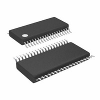
LTC3855IFE#PBF Linear Technology, LTC3855IFE#PBF Datasheet - Page 13

LTC3855IFE#PBF
Manufacturer Part Number
LTC3855IFE#PBF
Description
IC CTLR DC/DC MULTIPHASE 38SSOP
Manufacturer
Linear Technology
Series
PolyPhase®r
Type
Step-Down (Buck)r
Datasheet
1.LTC3855EUJPBF.pdf
(44 pages)
Specifications of LTC3855IFE#PBF
Internal Switch(s)
No
Synchronous Rectifier
Yes
Number Of Outputs
2
Voltage - Output
0.6 ~ 3.3 V, 0.6 ~ 12.5 V
Current - Output
25A
Frequency - Switching
250kHz ~ 770kHz
Voltage - Input
4.5 ~ 38 V
Operating Temperature
-40°C ~ 125°C
Mounting Type
Surface Mount
Package / Case
38-TSSOP Exposed Pad, 38-eTSSOP, 38-HTSSOP
Lead Free Status / RoHS Status
Lead free / RoHS Compliant
Power - Output
-
Available stocks
Company
Part Number
Manufacturer
Quantity
Price
operaTion
voltage below 0.6V (e.g., SGND). To select pulse-skipping
mode of operation, tie the MODE/PLLIN pin to INTV
select Burst Mode operation, float the MODE/PLLIN pin.
When a controller is enabled for Burst Mode operation,
the peak current in the inductor is set to approximately
one-third of the maximum sense voltage even though
the voltage on the I
average inductor current is higher than the load current,
the error amplifier EA will decrease the voltage on the I
pin. When the I
sleep signal goes high (enabling sleep mode) and both
external MOSFETs are turned off.
In sleep mode, the load current is supplied by the output
capacitor. As the output voltage decreases, the EA’s output
begins to rise. When the output voltage drops enough, the
sleep signal goes low, and the controller resumes normal
operation by turning on the top external MOSFET on the
next cycle of the internal oscillator. When a controller is
enabled for Burst Mode operation, the inductor current is
not allowed to reverse. The reverse current comparator
(I
the inductor current reaches zero, preventing it from
reversing and going negative. Thus, the controller oper-
ates in discontinuous operation. In forced continuous
operation, the inductor current is allowed to reverse at
light loads or under large transient conditions. The peak
inductor current is determined by the voltage on the I
pin. In this mode, the efficiency at light loads is lower than
in Burst Mode operation. However, continuous mode has
the advantages of lower output ripple and less interference
with audio circuitry.
When the MODE/PLLIN pin is connected to INTV
LTC3855 operates in PWM pulse-skipping mode at light
loads. At very light loads, the current comparator I
remain tripped for several cycles and force the external top
MOSFET to stay off for the same number of cycles (i.e.,
skipping pulses). The inductor current is not allowed to
reverse (discontinuous operation). This mode, like forced
continuous operation, exhibits low output ripple as well as
low audio noise and reduced RF interference as compared
to Burst Mode operation. It provides higher low current
efficiency than forced continuous mode, but not nearly as
high as Burst Mode operation.
REV
) turns off the bottom external MOSFET just before
TH
voltage drops below 0.5V, the internal
TH
pin indicates a lower value. If the
CMP
CC
CC
, the
may
. To
TH
TH
Multichip Operations (PHASMD and CLKOUT Pins)
The PHASMD pin determines the relative phases between
the internal controllers as well as the CLKOUT signal as
shown in Table 1. The phases tabulated are relative to
zero phase being defined as the rising edge of the clock
of phase 1.
Table 1.
PHASMD
Phase1
Phase2
CLKOUT
The CLKOUT signal can be used to synchronize additional
power stages in a multiphase power supply solution feeding
a single, high current output or separate outputs. Input
capacitance ESR requirements and efficiency losses are
substantially reduced because the peak current drawn from
the input capacitor is effectively divided by the number
of phases used and power loss is proportional to the
RMS current squared. A two stage, single output voltage
implementation can reduce input path power loss by 75%
and radically reduce the required RMS current rating of
the input capacitor(s).
Single Output Multiphase Operation
The LTC3855 can be used for single output multiphase
converters by making these connections
• Tie all of the I
• Tie all of the V
• Tie all of the TK/SS pins together
• Tie all of the RUN pins together
• Tie all of the ITEMP pins together
• Tie all of the I
For three or more phases, tie the inputs of the unused dif-
ferential amplifier(s) to ground. Examples of single output
multiphase converters are shown in Figures 20 to 23.
the same potential
TH
LIM
FB
GND
0°
180°
60°
pins together
pins together
pins together, or tie the I
FLOAT
0°
180°
90°
LTC3855
INTVcc
0°
240°
120°
LIM
pins to
3855f


