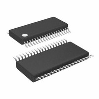
LTC3855IFE#PBF Linear Technology, LTC3855IFE#PBF Datasheet - Page 15

LTC3855IFE#PBF
Manufacturer Part Number
LTC3855IFE#PBF
Description
IC CTLR DC/DC MULTIPHASE 38SSOP
Manufacturer
Linear Technology
Series
PolyPhase®r
Type
Step-Down (Buck)r
Datasheet
1.LTC3855EUJPBF.pdf
(44 pages)
Specifications of LTC3855IFE#PBF
Internal Switch(s)
No
Synchronous Rectifier
Yes
Number Of Outputs
2
Voltage - Output
0.6 ~ 3.3 V, 0.6 ~ 12.5 V
Current - Output
25A
Frequency - Switching
250kHz ~ 770kHz
Voltage - Input
4.5 ~ 38 V
Operating Temperature
-40°C ~ 125°C
Mounting Type
Surface Mount
Package / Case
38-TSSOP Exposed Pad, 38-eTSSOP, 38-HTSSOP
Lead Free Status / RoHS Status
Lead free / RoHS Compliant
Power - Output
-
Available stocks
Company
Part Number
Manufacturer
Quantity
Price
operaTion
frequency of the LTC3855’s controllers can be selected
using the FREQ pin. If the MODE/PLLIN pin is not being
driven by an external clock source, the FREQ pin can be
used to program the controller’s operating frequency from
250kHz to 770kHz.
There is a precision 10µA current flowing out of the FREQ
pin, so the user can program the controller’s switching
frequency with a single resistor to SGND. A curve is
provided later in the application section showing the
relationship between the voltage on the FREQ pin and
switching frequency.
A phase-locked loop (PLL) is integrated on the LTC3855
to synchronize the internal oscillator to an external clock
source that is connected to the MODE/PLLIN pin. The
controller is operating in forced continuous mode when
it is synchronized.
The PLL loop filter network is integrated inside the LTC3855.
The phase-locked loop is capable of locking any frequency
within the range of 250kHz to 770kHz. The frequency setting
resistor should always be present to set the controller’s initial
switching frequency before locking to the external clock.
applicaTions inForMaTion
The Typical Application on the first page is a basic LTC3855
application circuit. LTC3855 can be configured to use either
DCR (inductor resistance) sensing or low value resistor
sensing. The choice between the two current sensing
schemes is largely a design trade-off between cost, power
consumption, and accuracy. DCR sensing is becoming
popular because it saves expensive current sensing resis-
tors and is more power efficient, especially in high current
applications. However, current sensing resistors provide
the most accurate current limits for the controller. Other
external component selection is driven by the load require-
ment, and begins with the selection of R
used) and inductor value. Next, the power MOSFETs are se-
lected. Finally, input and output capacitors are selected.
Current Limit Programming
The I
mum current limit of the controller. When I
grounded, floated or tied to INTV
LIM
pin is a tri-level logic input which sets the maxi-
CC
, the typical value
SENSE
LIM
(if R
is either
SENSE
is
for the maximum current sense threshold will be 30mV,
50mV or 75mV, respectively. The maximum current sense
threshold will be adjusted to values between these settings
by applying a voltage less than 0.5V to the ITEMP pin. See
the Operation section for more details.
Which setting should be used? For the best current limit
accuracy, use the 75mV setting. The 30mV setting will
allow for the use of very low DCR inductors or sense
resistors, but at the expense of current limit accuracy.
The 50mV setting is a good balance between the two. For
single output dual phase applications, use the 50mV or
75mV setting for optimal current sharing.
SENSE
The SENSE
comparators. The common mode input voltage range of
the current comparators is 0V to 12.5V. Both SENSE pins
are high impedance inputs with small base currents of
Power Good (PGOOD Pins)
When V
ence voltage, the PGOOD pin is pulled low. The PGOOD
pin is also pulled low when the RUN pin is below 1.2V or
when the LTC3855 is in the soft-start or tracking phase.
The PGOOD pin will flag power good immediately when
the V
However, there is an internal 20µs power bad mask when
V
PGOOD and only responds to its own channel signals.
The PGOOD pins are allowed to be pulled up by external
resistors to sources of up to 6V.
Output Overvoltage Protection
An overvoltage comparator, OV, guards against transient
overshoots (>10%) as well as other more serious condi-
tions that may overvoltage the output. In such cases, the
top MOSFET is turned off and the bottom MOSFET is turned
on until the overvoltage condition is cleared.
FB
goes out the ±10% window. Each channel has its own
FB
+
FB
pin is within the ±10% of the reference window.
and SENSE
pin voltage is not within ±10% of the 0.6V refer-
+
and SENSE
–
Pins
–
pins are the inputs to the current
LTC3855
3855f


