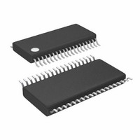
LTC3855IFE#PBF Linear Technology, LTC3855IFE#PBF Datasheet - Page 25

LTC3855IFE#PBF
Manufacturer Part Number
LTC3855IFE#PBF
Description
IC CTLR DC/DC MULTIPHASE 38SSOP
Manufacturer
Linear Technology
Series
PolyPhase®r
Type
Step-Down (Buck)r
Datasheet
1.LTC3855EUJPBF.pdf
(44 pages)
Specifications of LTC3855IFE#PBF
Internal Switch(s)
No
Synchronous Rectifier
Yes
Number Of Outputs
2
Voltage - Output
0.6 ~ 3.3 V, 0.6 ~ 12.5 V
Current - Output
25A
Frequency - Switching
250kHz ~ 770kHz
Voltage - Input
4.5 ~ 38 V
Operating Temperature
-40°C ~ 125°C
Mounting Type
Surface Mount
Package / Case
38-TSSOP Exposed Pad, 38-eTSSOP, 38-HTSSOP
Lead Free Status / RoHS Status
Lead free / RoHS Compliant
Power - Output
-
Available stocks
Company
Part Number
Manufacturer
Quantity
Price
Topside MOSFET Driver Supply (C
External bootstrap capacitors C
pins supply the gate drive voltages for the topside MOSFETs.
Capacitor C
external diode DB from INTV
When one of the topside MOSFETs is to be turned on,
the driver places the C
of the desired MOSFET. This enhances the MOSFET and
turns on the topside switch. The switch node voltage, SW,
rises to V
MOSFET on, the boost voltage is above the input supply:
V
C
citance of the topside MOSFET(s). The reverse break-
down of the external Schottky diode must be greater
than V
final arbiter is the total input current for the regulator. If
a change is made and the input current decreases, then
the efficiency has improved. If there is no change in input
current, then there is no change in efficiency.
Undervoltage Lockout
The LTC3855 has two functions that help protect the
controller in case of undervoltage conditions. A precision
UVLO comparator constantly monitors the INTV
to ensure that an adequate gate-drive voltage is present. It
locks out the switching action when INTV
To prevent oscillation when there is a disturbance on the
INTV
hysteresis.
applicaTions inForMaTion
due to the dropout voltage. Make sure the INTV
is at or exceeds the R
which is typically 4.5V for logic level devices.
BOOST
B
needs to be 100 times that of the total input capa-
CC
IN(MAX)
, the UVLO comparator has 600mV of precision
= V
IN
IN
B
and the BOOST pin follows. With the topside
in the Functional Diagram is charged though
+ V
. When adjusting the gate drive level, the
LTC3855
Figure 10. Setup for a 5V Input
INTVCC
INTV
V
DS(ON)
CC
IN
B
. The value of the boost capacitor
voltage across the gate source
CINTV
test voltage for the MOSFET
CC
4.7µF
B
CC
when the SW pin is low.
connected to the BOOST
B
R
1Ω
VIN
, DB)
+
CC
3855
is below 3.2V.
C
5V
IN
F07
CC
CC
voltage
voltage
Another way to detect an undervoltage condition is to
monitor the V
precision turn-on reference of 1.2V, one can use a resistor
divider to V
An extra 4.5µA of current flows out of the RUN pin once
the RUN pin voltage passes 1.2V. One can program the
hysteresis of the run comparator by adjusting the values
of the resistive divider. For accurate V
detection, V
C
The selection of C
ture and its impact on the worst-case RMS current drawn
through the input network (battery/fuse/capacitor). It can be
shown that the worst-case capacitor RMS current occurs
when only one controller is operating. The controller with
the highest (V
formula below to determine the maximum RMS capacitor
current requirement. Increasing the output current drawn
from the other controller will actually decrease the input
RMS ripple current from its maximum value. The out-of-
phase technique typically reduces the input capacitor’s RMS
ripple current by a factor of 30% to 70% when compared
to a single phase power supply solution.
In continuous mode, the source current of the top MOSFET
is a square wave of duty cycle (V
large voltage transients, a low ESR capacitor sized for the
maximum RMS current of one channel must be used. The
maximum RMS capacitor current is given by:
This formula has a maximum at V
I
for design because even significant deviations do not of-
fer much relief. Note that capacitor manufacturers’ ripple
current ratings are often based on only 2000 hours of life.
This makes it advisable to further derate the capacitor, or
to choose a capacitor rated at a higher temperature than
required. Several capacitors may be paralleled to meet
size or height requirements in the design. Due to the high
operating frequency of the LTC3855, ceramic capacitors
OUT
IN
C
and C
/2. This simple worst-case condition is commonly used
IN
Required I
OUT
IN
IN
to turn on the IC when V
Selection
OUT
IN
needs to be higher than 4.5V.
supply. Because the RUN pins have a
)(I
IN
RMS
is simplified by the 2-phase architec-
OUT
≈
) product needs to be used in the
I
MAX
V
IN
(
V
IN
OUT
OUT
= 2V
)
)/(V
(
IN
OUT
LTC3855
V
IN
IN
is high enough.
IN
, where I
– V
undervoltage
). To prevent
OUT
)
RMS
1/2
3855f
=


