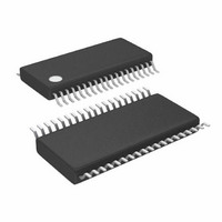
LTC3855EFE#PBF Linear Technology, LTC3855EFE#PBF Datasheet - Page 5

LTC3855EFE#PBF
Manufacturer Part Number
LTC3855EFE#PBF
Description
IC BUCK SYNC ADJ 25A DL 38TSSOP
Manufacturer
Linear Technology
Series
PolyPhase®r
Type
Step-Down (Buck)r
Datasheet
1.LTC3855EUJPBF.pdf
(44 pages)
Specifications of LTC3855EFE#PBF
Internal Switch(s)
No
Synchronous Rectifier
Yes
Number Of Outputs
2
Voltage - Output
0.6 ~ 3.3 V, 0.6 ~ 12.5 V
Current - Output
25A
Frequency - Switching
250kHz ~ 770kHz
Voltage - Input
4.5 ~ 38 V
Operating Temperature
-40°C ~ 85°C
Mounting Type
Surface Mount
Package / Case
38-TSSOP Exposed Pad, 38-eTSSOP, 38-HTSSOP
Primary Input Voltage
38V
No. Of Outputs
2
Output Voltage
12.5V
No. Of Pins
38
Operating Temperature Range
-40°C To +85°C
Msl
MSL 1 - Unlimited
Switching Frequency Max
770kHz
Rohs Compliant
Yes
Lead Free Status / RoHS Status
Lead free / RoHS Compliant
Power - Output
-
Available stocks
Company
Part Number
Manufacturer
Quantity
Price
elecTrical characTerisTics
SYMBOL
On Chip Driver
TG R
TG R
BG R
BG R
Note 1: Stresses beyond those listed under Absolute Maximum Ratings
may cause permanent damage to the device. Exposure to any Absolute
Maximum Rating condition for extended periods may affect device
reliability and lifetime.
Note 2: The LTC3855E is guaranteed to meet performance specifications
from 0°C to 85°C. Specifications over the –40°C to 85°C operating
junction temperature range are assured by design, characterization and
correlation with statistical process controls. The LTC3855I is guaranteed
to meet performance specifications over the full –40°C to 125°C operating
junction temperature range.
Note 3: T
dissipation P
Typical perForMance characTerisTics
junction temperature range (E-Grade), otherwise specifications are at T
LTC3855UJ: T
LTC3855FE: T
100
90
80
70
60
50
40
30
20
10
UP
DOWN
UP
DOWN
0
0.01
Efficiency vs Output Current
and Mode
J
OPERATION
Burst Mode
is calculated from the ambient temperature T
D
PARAMETER
TG Pull-Up R
TG Pull-Down R
BG Pull-Up R
BG Pull-Down R
according to the following formulas:
0.1
J
J
DCM
= T
= T
LOAD CURRENT (A)
A
A
CCM
+ (P
+ (P
D
CIRCUIT OF FIGURE 19
1
D
DS(ON)
DS(ON)
• 25°C/W)
• 33°C/W)
DS(ON)
DS(ON)
10
V
V
IN
OUT
= 12V
= 1.8V
3855 G23
100
CONDITIONS
TG High
TG Low
BG High
BG Low
A
100
90
80
70
60
50
40
30
20
10
and power
0
0.01
Efficiency vs Output Current
and Mode
OPERATION
Burst Mode
The
0.1
DCM
LOAD CURRENT (A)
l
CCM
denotes the specifications which apply over the full operating
1
CIRCUIT OF FIGURE 19
Note 4: The LTC3855 is tested in a feedback loop that servos V
specified voltage and measures the resultant V
Note 5: Dynamic supply current is higher due to the gate charge being
delivered at the switching frequency. See Applications Information.
Note 6: Rise and fall times are measured using 10% and 90% levels. Delay
times are measured using 50% levels.
Note 7: The minimum on-time condition is specified for an inductor
peak-to-peak ripple current ≥40% of I
Considerations in the Applications Information section).
Note 8: Guaranteed by design.
A
= 25°C. V
V
V
10
IN
OUT
= 12V
= 1.2V
3855 G24
IN
= 15V, V
100
RUN/SS
90
85
80
75
Full Load Efficiency and Power
Loss vs Input Voltage
5
CIRCUIT OF FIGURE 19
= 5V unless otherwise noted.
1.8V
POWER LOSS
MIN
MAX
1.2V
EFFICIENCY
INPUT VOLTAGE (V)
(see Minimum On-Time
10
1.8V
FB1,2
1.2V
TYP
2.6
1.5
2.4
1.1
.
LTC3855
15
MAX
ITH1,2
3855
G24
20
UNITS
to a
5
4
3
2
3855f
Ω
Ω
Ω
Ω


