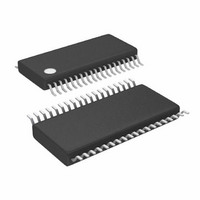
LTC3855EFE#PBF Linear Technology, LTC3855EFE#PBF Datasheet - Page 10

LTC3855EFE#PBF
Manufacturer Part Number
LTC3855EFE#PBF
Description
IC BUCK SYNC ADJ 25A DL 38TSSOP
Manufacturer
Linear Technology
Series
PolyPhase®r
Type
Step-Down (Buck)r
Datasheet
1.LTC3855EUJPBF.pdf
(44 pages)
Specifications of LTC3855EFE#PBF
Internal Switch(s)
No
Synchronous Rectifier
Yes
Number Of Outputs
2
Voltage - Output
0.6 ~ 3.3 V, 0.6 ~ 12.5 V
Current - Output
25A
Frequency - Switching
250kHz ~ 770kHz
Voltage - Input
4.5 ~ 38 V
Operating Temperature
-40°C ~ 85°C
Mounting Type
Surface Mount
Package / Case
38-TSSOP Exposed Pad, 38-eTSSOP, 38-HTSSOP
Primary Input Voltage
38V
No. Of Outputs
2
Output Voltage
12.5V
No. Of Pins
38
Operating Temperature Range
-40°C To +85°C
Msl
MSL 1 - Unlimited
Switching Frequency Max
770kHz
Rohs Compliant
Yes
Lead Free Status / RoHS Status
Lead free / RoHS Compliant
Power - Output
-
Available stocks
Company
Part Number
Manufacturer
Quantity
Price
pin FuncTions
LTC3855
BOOST1, BOOST2 (Pin 32, Pin 24/Pin 29, Pin 21): Boosted
Floating Driver Supplies. The (+) terminal of the bootstrap
capacitors connect to these pins. These pins swing from a
diode voltage drop below INTV
TG1, TG2 (Pin 33, Pin 23/Pin 30, Pin 20): Top Gate
Driver Outputs. These are the outputs of floating drivers
with a voltage swing equal to INTV
the switch nodes voltages.
SW1, SW2 (Pin 34, Pin 22/Pin 31, Pin 19): Switch Node
Connections to Inductors. Voltage swing at these pins
is from a Schottky diode (external) voltage drop below
ground to V
PHASMD (Pin 36/Pin 33): This pin can be tied to SGND,
tied to INTV
relative phases between the internal controllers as well
as the phasing of the CLKOUT signal. See Table 1 in the
Operation section.
CLKOUT (Pin 35/Pin 32): Clock output with phase change-
able by PHASMD to enable usage of multiple LTC3855 in
multiphase systems.
0
IN
CC
.
or left floating. This pin determines the
(FE38/UJ40)
CC
up to V
CC
superimposed on
IN
+ INTV
CC
.
MODE/PLLIN (Pin 37/Pin 34): This is a dual purpose pin.
When external frequency synchronization is not used,
this pin selects the operating mode. The pin can be tied
to SGND, tied to INTV
forced continuous mode. INTV
mode. Floating enables Burst Mode operation. For external
sync, apply a clock signal to this pin. Both channels will
go into forced continuous mode and the internal PLL will
synchronize the internal oscillator to the clock. The PLL
compensation network is integrated into the IC.
FREQ (Pin 38/Pin 35): There is a precision 10µA current
flowing out of this pin. A resistor to ground sets a voltage
which in turn programs the frequency. Alternatively, this
pin can be driven with a DC voltage to vary the frequency
of the internal oscillator.
SGND (Exposed Pad Pin 39/ Pin 4, Exposed Pad Pin 41):
Signal Ground. All small-signal components and com-
pensation components should connect to this ground,
which in turn connects to PGND at one point. Exposed
pad must be soldered to PCB, providing a local ground
for the control components of the IC, and be tied to the
PGND pin under the IC.
CC
or left floating. SGND enables
CC
enables pulse-skipping
3855f


