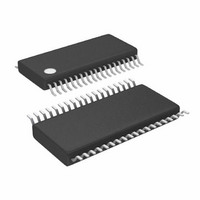
LTC3855EFE#PBF Linear Technology, LTC3855EFE#PBF Datasheet - Page 20

LTC3855EFE#PBF
Manufacturer Part Number
LTC3855EFE#PBF
Description
IC BUCK SYNC ADJ 25A DL 38TSSOP
Manufacturer
Linear Technology
Series
PolyPhase®r
Type
Step-Down (Buck)r
Datasheet
1.LTC3855EUJPBF.pdf
(44 pages)
Specifications of LTC3855EFE#PBF
Internal Switch(s)
No
Synchronous Rectifier
Yes
Number Of Outputs
2
Voltage - Output
0.6 ~ 3.3 V, 0.6 ~ 12.5 V
Current - Output
25A
Frequency - Switching
250kHz ~ 770kHz
Voltage - Input
4.5 ~ 38 V
Operating Temperature
-40°C ~ 85°C
Mounting Type
Surface Mount
Package / Case
38-TSSOP Exposed Pad, 38-eTSSOP, 38-HTSSOP
Primary Input Voltage
38V
No. Of Outputs
2
Output Voltage
12.5V
No. Of Pins
38
Operating Temperature Range
-40°C To +85°C
Msl
MSL 1 - Unlimited
Switching Frequency Max
770kHz
Rohs Compliant
Yes
Lead Free Status / RoHS Status
Lead free / RoHS Compliant
Power - Output
-
Available stocks
Company
Part Number
Manufacturer
Quantity
Price
LTC3855
applicaTions inForMaTion
greater than 0.2V for duty cycles of 25% or more, oth-
erwise temperature correction may not occur at elevated
ambients. For the most accurate temperature detection,
place the thermistors next to the inductors as shown in
Figure 7. Take care to keep the ITEMP pins away from the
switch nodes.
Slope Compensation and Inductor Peak Current
Slope compensation provides stability in constant-
frequency architectures by preventing subharmonic oscil-
lations at high duty cycles. It is accomplished internally by
adding a compensating ramp to the inductor current signal
at duty cycles in excess of 40%. Normally, this results in
a reduction of maximum inductor peak current for duty
cycles > 40%. However, the LTC3855 uses a scheme that
counteracts this compensating ramp, which allows the
0
CONNECT TO
NETWORK
(7a) Dual Output Dual Phase DCR Sensing Application
ITEMP1
Figure 5. Resistance Versus Temperature for
ITEMP Pin Network and the 100k NTC
R
10000
NTC1
1000
100
10
1
–40
GND
Figure 7. Thermistor Locations. Place Thermistor Next to Inductor(s) for Accurate Sensing of the Inductor
Temperature, but Keep the ITEMP Pins Away from the Switch Nodes and Gate Drive Traces
RITMP
R
R
100k NTC
–20
S
P
= 20k
= 43.2k
INDUCTOR TEMPERATURE (°C)
V
SW1
OUT1
THERMISTOR RESISTANCE
R
B = 4334 for 25°C/100°C
L1
0
O
= 100k, T
20
40
O
= 25°C
60
V
SW2
OUT2
L2
80
3855
F07a
100
3855
GND
120
F05
R
NTC2
CONNECT TO
ITEMP2
NETWORK
maximum inductor peak current to remain unaffected
throughout all duty cycles.
Inductor Value Calculation
Given the desired input and output voltages, the inductor
value and operating frequency f
inductor’s peak-to-peak ripple current:
Lower ripple current reduces core losses in the inductor,
ESR losses in the output capacitors, and output voltage
ripple. Thus, highest efficiency operation is obtained at
low frequency with a small ripple current. Achieving this,
however, requires a large inductor.
I
RIPPLE
Figure 6. Worst Case I
Curve with and without NTC Temperature Compensation
(7b) Single Output Dual Phase DCR Sensing Application
=
25
20
15
10
5
0
–40
V
V
OUT
NOMINAL I
R
R
NTC THERMISTOR:
R
T
B = 4334
O
IN
S
P
O
–20
= 25°C
= 20k
= 43.2k
= 100k
INDUCTOR TEMPERATURE (°C)
V
SW1
V
OUT
L1
0
MAX
IN
f
OSC
MAX
– V
20
• L
Versus Inductor Temperature
OUT
R
UNCORRECTED I
CORRECTED I
40
NTC
OSC
60
SW2
80
directly determine the
L2
MAX
3855
MAX
100
F07b
3855
F06
120
3855f


