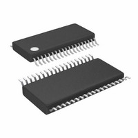
LTC3855EFE#PBF Linear Technology, LTC3855EFE#PBF Datasheet - Page 22

LTC3855EFE#PBF
Manufacturer Part Number
LTC3855EFE#PBF
Description
IC BUCK SYNC ADJ 25A DL 38TSSOP
Manufacturer
Linear Technology
Series
PolyPhase®r
Type
Step-Down (Buck)r
Datasheet
1.LTC3855EUJPBF.pdf
(44 pages)
Specifications of LTC3855EFE#PBF
Internal Switch(s)
No
Synchronous Rectifier
Yes
Number Of Outputs
2
Voltage - Output
0.6 ~ 3.3 V, 0.6 ~ 12.5 V
Current - Output
25A
Frequency - Switching
250kHz ~ 770kHz
Voltage - Input
4.5 ~ 38 V
Operating Temperature
-40°C ~ 85°C
Mounting Type
Surface Mount
Package / Case
38-TSSOP Exposed Pad, 38-eTSSOP, 38-HTSSOP
Primary Input Voltage
38V
No. Of Outputs
2
Output Voltage
12.5V
No. Of Pins
38
Operating Temperature Range
-40°C To +85°C
Msl
MSL 1 - Unlimited
Switching Frequency Max
770kHz
Rohs Compliant
Yes
Lead Free Status / RoHS Status
Lead free / RoHS Compliant
Power - Output
-
Available stocks
Company
Part Number
Manufacturer
Quantity
Price
LTC3855
applicaTions inForMaTion
The MOSFET power dissipations at maximum output
current are given by:
where d is the temperature dependency of R
R
at the MOSFET’s Miller threshold voltage. V
typical MOSFET minimum threshold voltage.
Both MOSFETs have I
equation includes an additional term for transition losses,
which are highest at high input voltages. For V
the high current efficiency generally improves with larger
MOSFETs, while for V
increase to the point that the use of a higher R
with lower C
synchronous MOSFET losses are greatest at high input
voltage when the top switch duty factor is low or during
a short-circuit when the synchronous switch is on close
to 100% of the period.
The term (1 + d) is generally given for a MOSFET in the
form of a normalized R
d = 0.005/°C can be used as an approximation for low
voltage MOSFETs.
The optional Schottky diodes conduct during the dead time
between the conduction of the two power MOSFETs. These
prevent the body diodes of the bottom MOSFETs from turn-
ing on, storing charge during the dead time and requiring
a reverse recovery period that could cost as much as 3%
in efficiency at high V
a good compromise for both regions of operation due to
DR
P
P
SYNC
MAIN
(approximately 2Ω) is the effective driver resistance
=
=
( )
V
V
V
V
MILLER
IN
INTVCC
V
IN
OUT
IN
–
2
V
IN
(
V
I
I
OUT
MAX
MAX
actually provides higher efficiency. The
–
2 2
1
2
IN
V
R losses while the topside N-channel
IN
(
)
TH MIN
> 20V the transition losses rapidly
DS(ON)
. A 1A to 3A Schottky is generally
I
2
MAX
(
(
R
(
1 d
DR
+
) )
)
2
)(
vs Temperature curve, but
+
)
(
C
R
1 d R
V
+
MILLER
DS ON
T T H MIN
(
)
(
1
DS ON
)
+
)
)
(
•
•
TH(MIN)
DS(ON)
f
)
OSC
DS(ON)
IN
device
< 20V
is the
and
the relatively small average current. Larger diodes result
in additional transition losses due to their larger junction
capacitance. A Schottky diode in parallel with the bottom
FET may also provide a modest improvement in Burst
Mode efficiency.
Soft-Start and Tracking
The LTC3855 has the ability to either soft-start by itself
with a capacitor or track the output of another channel or
external supply. When one particular channel is configured
to soft-start by itself, a capacitor should be connected to
its TK/SS pin. This channel is in the shutdown state if its
RUN pin voltage is below 1.2V. Its TK/SS pin is actively
pulled to ground in this shutdown state.
Once the RUN pin voltage is above 1.2V, the channel pow-
ers up. A soft-start current of 1.2µA then starts to charge
its soft-start capacitor. Note that soft-start or tracking is
achieved not by limiting the maximum output current of
the controller but by controlling the output ramp voltage
according to the ramp rate on the TK/SS pin. Current
foldback is disabled during this phase to ensure smooth
soft-start or tracking. The soft-start or tracking range is
defined to be the voltage range from 0V to 0.6V on the
TK/SS pin. The total soft-start time can be calculated as:
Regardless of the mode selected by the MODE/PLLIN pin,
the regulator will always start in pulse-skipping mode
up to TK/SS = 0.5V. Between TK/SS = 0.5V and 0.54V, it
will operate in forced continuous mode and revert to the
selected mode once TK/SS > 0.54V. The output ripple
is minimized during the 40mV forced continuous mode
window ensuring a clean PGOOD signal.
When the channel is configured to track another supply,
the feedback voltage of the other supply is duplicated by
a resistor divider and applied to the TK/SS pin. Therefore,
the voltage ramp rate on this pin is determined by the
ramp rate of the other supply’s voltage. Note that the small
soft-start capacitor charging current is always flowing,
t
SOFTSTART
= 0.6 •
1.2µA
C
SS
3855f


