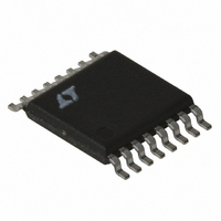
LT3825EFE#TRPBF Linear Technology, LT3825EFE#TRPBF Datasheet - Page 23

LT3825EFE#TRPBF
Manufacturer Part Number
LT3825EFE#TRPBF
Description
IC CNTRLR SYNC 16-TSSOP
Manufacturer
Linear Technology
Type
Flybackr
Datasheet
1.LT3825EFEPBF.pdf
(32 pages)
Specifications of LT3825EFE#TRPBF
Internal Switch(s)
No
Synchronous Rectifier
Yes
Number Of Outputs
1
Frequency - Switching
50kHz ~ 250kHz
Voltage - Input
12 ~ 18 V
Operating Temperature
-40°C ~ 125°C
Mounting Type
Surface Mount
Package / Case
16-TSSOP Exposed Pad, 16-eTSSOP, 16-HTSSOP
Power - Output
60W
Lead Free Status / RoHS Status
Lead free / RoHS Compliant
Current - Output
-
Voltage - Output
-
Available stocks
Company
Part Number
Manufacturer
Quantity
Price
APPLICATIONS INFORMATION
For each secondary-side power MOSFET RMS current is
given by:
Calculate MOSFET power dissipation next. Because the
primary-side power MOSFET operates at high V
tion power loss term is included for accuracy. C
the most critical parameter in determining the transition
loss, but is not directly specified on the data sheets.
C
on most MOSFET data sheets (Figure 6).
The flat portion of the curve is the result of the Miller
(gate-to-drain) capacitance as the drain voltage drops.
The Miller capacitance is computed as:
The curve is done for a given V
for different V
computed C
the curve specified V
With C
MOSFET power dissipation:
MILLER
I
P
C
V
RMS SEC
DPRI
IN(MAX)
MILLER
MILLER
(
is calculated from the gate charge curve included
= I
)
RMS(PRI)
=
MILLER
•
=
determined, calculate the primary-side power
DS
P
Q
V
DC
IN(MAX)
GS
B
Figure 6. Gate Charge Curve
voltages are estimated by multiplying the
V
1
–
DS
MIN
–
I
Q
by the ratio of the application V
OUT
2
DC
Q
a
DS
A
A
GATE CHARGE (Q
• R
MILLER EFFECT
MAX
.
• R
DS(ON)
DR
•
DS
(
V
1+ δ
G
Q
GATE(MAX)
b
. The Miller capacitance
)
B
C
)
3825 F06
MILLER
+
– V
DS
TH
, a transi-
MILLER
• f
DS
OSC
to
is
where:
(1 + δ) is generally given for a MOSFET in the form of a
normalized R
have a curve, use δ = 0.005/°C • ΔT for low voltage
MOSFETs.
The secondary-side power MOSFETs typically operate
at substantially lower V
losses. The dissipation is calculated using:
With power dissipation known, the MOSFETs’ junction
temperatures are obtained from the equation:
where T
junction-to-ambient thermal resistance.
Once you have T
δ and power dissipations until convergence.
Gate Drive Node Consideration
The PG and SG gate drivers are strong drives to minimize
gate drive rise and fall times. This improves efficiency
but the high frequency components of these signals can
cause problems. Keep the traces short and wide to reduce
parasitic inductance.
The parasitic inductance creates an LC tank with the
MOSFET gate capacitance. In less than ideal layouts, a
series resistance of 5Ω or more may help to dampen the
ringing at the expense of slightly slower rise and fall times
and efficiency.
The LT3825 gate drives will clamp the max gate voltage
to roughly 7.4V, so you can safely use MOSFETs with max
V
GS
R
V
f
V
P
T
OSC
TH
J
GATE(MAX)
D(SEC)
DR
of 10V or larger.
= T
is the MOSFET gate threshold voltage
is the gate driver resistance (≈10Ω)
A
is the operating frequency
A
is the ambient temperature and θ
+ P
= I
RMS(SEC)
DS(ON)
D
= 7.5V for this part
• θ
J
, iterate your calculations recomputing
JA
vs temperature curve. If you don’t
2
DS
• R
, so you can neglect transition
DS(ON)
(1 + δ)
JA
is the MOSFET
LT3825
23
3825fc


