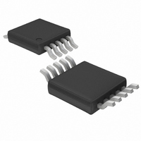
LTC1871IMS-1#TRPBF Linear Technology, LTC1871IMS-1#TRPBF Datasheet - Page 28

LTC1871IMS-1#TRPBF
Manufacturer Part Number
LTC1871IMS-1#TRPBF
Description
IC CONTRLR CURRENT MODE 10-MSOP
Manufacturer
Linear Technology
Type
Step-Up (Boost), Flyback, Sepicr
Datasheet
1.LTC1871EMS-1PBF.pdf
(36 pages)
Specifications of LTC1871IMS-1#TRPBF
Internal Switch(s)
No
Synchronous Rectifier
No
Number Of Outputs
1
Voltage - Output
1.23 ~ 72 V
Current - Output
50mA
Frequency - Switching
50kHz ~ 1MHz
Voltage - Input
2.5 ~ 36 V
Operating Temperature
-40°C ~ 125°C
Mounting Type
Surface Mount
Package / Case
10-MSOP, Micro10™, 10-uMAX, 10-uSOP
Lead Free Status / RoHS Status
Lead free / RoHS Compliant
Power - Output
-
Available stocks
Company
Part Number
Manufacturer
Quantity
Price
LTC1871-1
APPLICATIONS INFORMATION
choice is AVX TPS series of surface mount tantalum. Also,
ceramic capacitors are now available with extremely low
ESR, ESL and high ripple current ratings.
SEPIC Converter: Input Capacitor Selection
The input capacitor of a SEPIC converter is less critical
than the output capacitor due to the fact that an inductor
is in series with the input and the input current waveform
is triangular in shape. The input voltage source impedance
determines the size of the input capacitor which is typi-
cally in the range of 10μF to 100μF . A low ESR capacitor
is recommended, although it is not as critical as for the
output capacitor.
The RMS input capacitor ripple current for a SEPIC con-
verter is:
Please note that the input capacitor can see a very high
surge current when a battery is suddenly connected to
the input of the converter and solid tantalum capacitors
can fail catastrophically under these conditions. Be sure
to specify surge-tested capacitors!
SEPIC Converter: Selecting the DC Coupling Capacitor
The coupling capacitor C1 in Figure 16 sees nearly a rectan-
gular current waveform as shown in Figure 17. During the
switch off-time the current through C1 is I
approximately – I
waveform creates a triangular ripple voltage on C1:
The maximum voltage on C1 is then:
28
I
V
RMS(CIN)
C1(MAX)
V
C1(P P)
= V
=
=
IN
I
O(MAX)
1
12
C1• f
O
+
fl ows during the on-time. This current
• I
V
C1(P P)
•
L
2
V
IN
+ V
V
O
O
+ V
D
O
(V
O
/V
IN
) while
which is typically close to V
through C1 is:
The value chosen for the DC coupling capacitor normally
starts with the minimum value that will satisfy 1) the RMS
current requirement and 2) the peak voltage requirement
(typically close to V
capacitors work well here.
SEPIC Converter Design Example
The design example given here will be for the circuit shown
in Figure 18. The input voltage is 5V to 15V and the output
is 12V at a maximum load current of 1.5A (2A peak).
1. The duty cycle range is:
2. The operating mode chosen is pulse skipping, so the
3. The operating frequency is chosen to be 300kHz to
4. An inductor ripple current of 40% is chosen, so the peak
MODE/SYNC pin is shorted to INTV
reduce the size of the inductors; the resistor from the
FREQ pin to ground is 80k.
input current (which is also the minimum saturation
current) is:
The inductor ripple current is:
I
I
RMS(C1)
L1(PEAK)
I
L
D =
= •I
= 0.4 • 1.5 •
V
=I
= 1+
= 1+
IN
O(MAX)
O(MAX)
V
+ V
O
+ V
O
0.4
2
1– 0.714
2
+ V
•
IN
D
0.714
•
1– D
). Low ESR ceramic and tantalum
•I
D
D
• 1.5 •
O(MAX)
V
MAX
V
IN(MIN)
O
MAX
= 45.5% to 71.4%
+ V
= 1.5A
IN(MAX)
12 + 0.5
D
•
V
V
5
IN(MIN)
O
+ V
. The ripple current
CC
D
= 4.5A
.
18711fb


