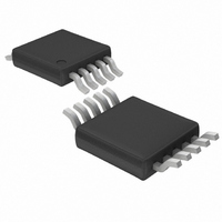
LTC1871IMS-1#TRPBF Linear Technology, LTC1871IMS-1#TRPBF Datasheet - Page 20

LTC1871IMS-1#TRPBF
Manufacturer Part Number
LTC1871IMS-1#TRPBF
Description
IC CONTRLR CURRENT MODE 10-MSOP
Manufacturer
Linear Technology
Type
Step-Up (Boost), Flyback, Sepicr
Datasheet
1.LTC1871EMS-1PBF.pdf
(36 pages)
Specifications of LTC1871IMS-1#TRPBF
Internal Switch(s)
No
Synchronous Rectifier
No
Number Of Outputs
1
Voltage - Output
1.23 ~ 72 V
Current - Output
50mA
Frequency - Switching
50kHz ~ 1MHz
Voltage - Input
2.5 ~ 36 V
Operating Temperature
-40°C ~ 125°C
Mounting Type
Surface Mount
Package / Case
10-MSOP, Micro10™, 10-uMAX, 10-uSOP
Lead Free Status / RoHS Status
Lead free / RoHS Compliant
Power - Output
-
Available stocks
Company
Part Number
Manufacturer
Quantity
Price
LTC1871-1
APPLICATIONS INFORMATION
3. The losses in the inductor are simply the DC input cur-
4. Losses in the boost diode. The power dissipation in the
5. Other losses, including C
Checking Transient Response
The regulator loop response can be verifi ed by looking at
the load transient response. Switching regulators generally
take several cycles to respond to an instantaneous step
in resistive load current. When the load step occurs, V
immediately shifts by an amount equal to (ΔI
and then C
the direction of the load step) as shown in Figure 13. The
regulator feedback loop acts on the resulting error amp
output signal to return V
this recovery time, V
ringing that would indicate a stability problem.
20
dissipated in this resistor would be 514mW at maxi-
mum output current. Assuming an effi ciency of 90%,
this sense resistor power dissipation represents 1.3%
of the overall input power. In other words, for this ap-
plication, the use of V
effi ciency by approximately 1.3%.
For more details regarding the various terms in these
equations, please refer to the section Boost Converter:
Power MOSFET Selection.
rent squared times the winding resistance. Expressing
this loss as a function of the output current yields:
boost diode is:
The boost diode can be a major source of power loss
in a boost converter. For the 3.3V input, 5V output at
7A example given above, a Schottky diode with a 0.4V
forward voltage would dissipate 2.8W, which represents
7% of the input power. Diode losses can become signifi -
cant at low output voltages where the forward voltage
is a signifi cant percentage of the output voltage.
inductor core losses, generally account for less than
2% of the total additional loss.
P
P
R(WINDING)
DIODE
O
begins to charge or discharge (depending on
= I
O(MAX)
=
O
1– D
I
can be monitored for overshoot or
• V
O(MAX)
O
DS
D
to its steady-state value. During
MAX
IN
sensing would increase the
and C
2
• R
O
W
ESR dissipation and
LOAD
)(ESR),
O
A second, more severe transient can occur when con-
necting loads with large (> 1μF) supply bypass capacitors.
The discharged bypass capacitors are effectively put in
parallel with C
V
this problem if the load switch resistance is low and it is
driven quickly. The only solution is to limit the rise time
of the switch drive in order to limit the inrush current
di/dt to the load.
Boost Converter Design Example
The design example given here will be for the circuit shown
in Figure 1. The input voltage is 3.3V, and the output is 5V
at a maximum load current of 7A (10A peak).
1. The duty cycle is:
2. Pulse-skip operation is chosen so the MODE/SYNC pin
3. The operating frequency is chosen to be 300kHz to
4. An inductor ripple current of 40% of the maximum load
O
. No regulator can deliver enough current to prevent
is shorted to INTV
reduce the size of the inductor. From Figure 5, the
resistor from the FREQ pin to ground is 80k.
current is chosen, so the peak input current (which is
also the minimum saturation current) is:
I
D =
100mV/DIV
IN(PEAK)
Figure 13. Load Transient Response for a 3.3V Input,
5V Output Boost Converter Application, 0.7A to 7A Step
V
OUT
2V/DIV
I
(AC)
OUT
V
O
V
+ V
= 1+
O
O
+ V
D
, causing a nearly instantaneous drop in
– V
D
2
IN
CC
•
.
1– D
I
=
O(MAX)
100μs/DIV
5 + 0.4 – 3.3
MAX
5 + 0.4
V
V
MODE/SYNC = INTV
(PULSE-SKIP MODE)
IN
OUT
= 1.2 •
= 3.3V
= 5V
= 38.9%
1– 0.39
18711 F13
7
CC
= 13.8A
18711fb


