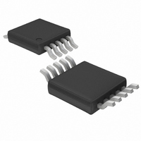
LTC1871IMS-1#TRPBF Linear Technology, LTC1871IMS-1#TRPBF Datasheet - Page 15

LTC1871IMS-1#TRPBF
Manufacturer Part Number
LTC1871IMS-1#TRPBF
Description
IC CONTRLR CURRENT MODE 10-MSOP
Manufacturer
Linear Technology
Type
Step-Up (Boost), Flyback, Sepicr
Datasheet
1.LTC1871EMS-1PBF.pdf
(36 pages)
Specifications of LTC1871IMS-1#TRPBF
Internal Switch(s)
No
Synchronous Rectifier
No
Number Of Outputs
1
Voltage - Output
1.23 ~ 72 V
Current - Output
50mA
Frequency - Switching
50kHz ~ 1MHz
Voltage - Input
2.5 ~ 36 V
Operating Temperature
-40°C ~ 125°C
Mounting Type
Surface Mount
Package / Case
10-MSOP, Micro10™, 10-uMAX, 10-uSOP
Lead Free Status / RoHS Status
Lead free / RoHS Compliant
Power - Output
-
Available stocks
Company
Part Number
Manufacturer
Quantity
Price
APPLICATIONS INFORMATION
from a lithium-ion battery or a 3.3V logic supply), then
sublogic-level threshold MOSFETs should be used.
Pay close attention to the BV
MOSFETs relative to the maximum actual switch voltage in
the application. Many logic-level devices are limited to 30V
or less, and the switch node can ring during the turn-off of
the MOSFET due to layout parasitics. Check the switching
waveforms of the MOSFET directly across the drain and
source terminals using the actual PC board layout (not
just on a lab breadboard!) for excessive ringing.
During the switch on-time, the control circuit limits the
maximum voltage drop across the power MOSFET to about
150mV (at low duty cycle). The peak inductor current
is therefore limited to 150mV/R
between the maximum load current, duty cycle and the
R
The V
cycle, and is reduced to about 100mV at a duty cycle of
92% due to slope compensation, as shown in Figure 10.
The ρ
the R
Figure 11 illustrates the variation of normalized R
over temperature for a typical power MOSFET.
DS(ON)
Figure 10. Maximum SENSE Threshold Voltage vs Duty Cycle
R
DS(ON)
DS(ON)
T
SENSE(MAX)
term accounts for the temperature coeffi cient of
of the power MOSFET is:
200
100
150
50
of the MOSFET, which is typically 0.4%/°C.
0
V
0
SENSE(MAX)
term is typically 150mV at low duty
0.2
DUTY CYCLE
0.4
•
1+
DSS
0.5
DS(ON)
2
1– D
specifi cations for the
•I
0.8
O(MAX)
. The relationship
MAX
18711 F10
1.0
•
T
DS(ON)
Another method of choosing which power MOSFET to
use is to check what the maximum output current is for a
given R
in discrete values.
It is worth noting that the 1 – D
I
wide input range to experience a dramatic range of maxi-
mum input and output current. This should be taken into
consideration in applications where it is important to limit
the maximum current drawn from the input supply.
Calculating Power MOSFET Switching and Conduction
Losses and Junction Temperatures
In order to calculate the junction temperature of the
power MOSFET, the power dissipated by the device must
be known. This power dissipation is a function of the
duty cycle, the load current and the junction temperature
itself (due to the positive temperature coeffi cient of its
R
required to determine a reasonably accurate value. Since
the controller is using the MOSFET as both a switching
and a sensing element, care should be taken to ensure
that the converter is capable of delivering the required
load current over all operating conditions (line voltage
and temperature), and for the worst-case specifi cations
O(MAX)
DS(ON)
I
O(MAX)
DS(ON)
). As a result, some iterative calculation is normally
and R
Figure 11. Normalized R
= V
2.0
1.0
0.5
1.5
0
, since MOSFET on-resistances are available
–50
SENSE(MAX)
DS(ON)
JUNCTION TEMPERATURE (°C)
can cause boost converters with a
0
•
1+
50
DS(ON)
MAX
2
1– D
vs Temperature
LTC1871-1
• R
relationship between
100
DS(ON)
MAX
18711 F11
150
•
T
15
18711fb


