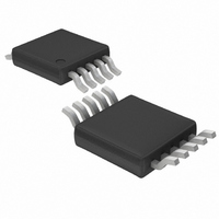
LTC1871IMS-1#TRPBF Linear Technology, LTC1871IMS-1#TRPBF Datasheet - Page 13

LTC1871IMS-1#TRPBF
Manufacturer Part Number
LTC1871IMS-1#TRPBF
Description
IC CONTRLR CURRENT MODE 10-MSOP
Manufacturer
Linear Technology
Type
Step-Up (Boost), Flyback, Sepicr
Datasheet
1.LTC1871EMS-1PBF.pdf
(36 pages)
Specifications of LTC1871IMS-1#TRPBF
Internal Switch(s)
No
Synchronous Rectifier
No
Number Of Outputs
1
Voltage - Output
1.23 ~ 72 V
Current - Output
50mA
Frequency - Switching
50kHz ~ 1MHz
Voltage - Input
2.5 ~ 36 V
Operating Temperature
-40°C ~ 125°C
Mounting Type
Surface Mount
Package / Case
10-MSOP, Micro10™, 10-uMAX, 10-uSOP
Lead Free Status / RoHS Status
Lead free / RoHS Compliant
Power - Output
-
Available stocks
Company
Part Number
Manufacturer
Quantity
Price
APPLICATIONS INFORMATION
Application Circuits
A basic LTC1871-1 application circuit is shown in
Figure 1. External component selection is driven by the
characteristics of the load and the input supply. The
fi rst topology to be analyzed will be the boost converter,
followed by SEPIC (single ended primary inductance
converter).
Boost Converter: Duty Cycle Considerations
For a boost converter operating in a continuous conduction
mode (CCM), the duty cycle of the main switch is:
where V
converters where the input voltage is close to the output
voltage, the duty cycle is low and for converters that develop
a high output voltage from a low voltage input supply,
the duty cycle is high. The maximum output voltage for a
boost converter operating in CCM is:
The maximum duty cycle capability of the LTC1871-1 is
typically 92%. This allows the user to obtain high output
voltages from low input supply voltages.
Boost Converter: The Peak and Average Input Currents
The control circuit in the LTC1871-1 is measuring the input
current (either by using the R
or by using a sense resistor in the MOSFET source), so
the output current needs to be refl ected back to the input
in order to dimension the power MOSFET properly. Based
on the fact that, ideally, the output power is equal to the
input power, the maximum average input current is:
The peak input current is:
D =
I
I
V
IN(MAX)
IN(PEAK)
O(MAX)
D
V
O
is the forward voltage of the boost diode. For
=
V
+ V
=
= 1+
O
1– D
(
I
+ V
1– D
O(MAX)
D
V
IN(MIN)
– V
D
MAX
2
MAX
IN
•
)
1– D
I
O(MAX)
– V
MAX
D
DS(ON)
of the power MOSFET
The maximum duty cycle, D
minimum V
Boost Converter: Ripple Current ΔI
The constant ‘χ’ in the equation above represents the
percentage peak-to-peak ripple current in the inductor,
relative to its maximum value. For example, if 30% ripple
current is chosen, then χ = 0.30, and the peak current is
15% greater than the average.
For a current mode boost regulator operating in CCM,
slope compensation must be added for duty cycles above
50% in order to avoid subharmonic oscillation. For the
LTC1871-1, this ramp compensation is internal. Having an
internally fi xed ramp compensation waveform, however,
does place some constraints on the value of the inductor
and the operating frequency. If too large an inductor is
used, the resulting current ramp (ΔI
to the internal ramp compensation (at duty cycles above
50%), and the converter operation will approach voltage
mode (ramp compensation reduces the gain of the current
loop). If too small an inductor is used, but the converter
is still operating in CCM (near critical conduction mode),
the internal ramp compensation may be inadequate to
prevent subharmonic oscillation. To ensure good current
mode gain and avoid subharmonic oscillation, it is recom-
mended that the ripple current in the inductor fall in the
range of 20% to 40% of the maximum average current.
For example, if the maximum average input current is
1A, choose a ΔI
between 0.2 and 0.4.
Boost Converter: Inductor Selection
Given an operating input voltage range, and having chosen
the operating frequency and ripple current in the inductor,
the inductor value can be determined using the following
equation:
where:
L =
I
L
V
= •
IN(MIN)
I
L
IN
• f
1– D
I
.
O(MAX)
• D
L
MAX
between 0.2A and 0.4A, and a value ‘χ’
MAX
MAX
, should be calculated at
L
LTC1871-1
) will be small relative
L
and the ‘χ’ Factor
13
18711fb


