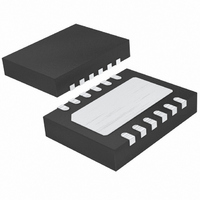
LTC3458EDE#PBF Linear Technology, LTC3458EDE#PBF Datasheet - Page 8

LTC3458EDE#PBF
Manufacturer Part Number
LTC3458EDE#PBF
Description
IC CONV DC/DC SYNC BOOST 12DFN
Manufacturer
Linear Technology
Type
Step-Up (Boost)r
Datasheet
1.LTC3458EDE.pdf
(16 pages)
Specifications of LTC3458EDE#PBF
Internal Switch(s)
Yes
Synchronous Rectifier
Yes
Number Of Outputs
1
Voltage - Output
2 ~ 7.5 V
Current - Output
1.4A
Frequency - Switching
1.5MHz
Voltage - Input
1.5 ~ 6 V
Operating Temperature
-40°C ~ 85°C
Mounting Type
Surface Mount
Package / Case
12-DFN
Dc To Dc Converter Type
Step Up
Pin Count
12
Input Voltage
6V
Output Voltage
2 to 7.5V
Switching Freq
1.15MHz
Output Current
1.6A
Efficiency
93%
Package Type
DFN EP
Output Type
Adjustable
Switching Regulator
Yes
Mounting
Surface Mount
Input Voltage (min)
1.5V
Operating Temp Range
-40C to 85C
Operating Temperature Classification
Industrial
Primary Input Voltage
6V
No. Of Outputs
1
No. Of Pins
12
Operating Temperature Range
-40°C To +85°C
Msl
MSL 1 - Unlimited
Rohs Compliant
Yes
Lead Free Status / RoHS Status
Lead free / RoHS Compliant
Power - Output
-
Lead Free Status / Rohs Status
Compliant
Available stocks
Company
Part Number
Manufacturer
Quantity
Price
BLOCK DIAGRA
LTC3458
APPLICATIO S I FOR ATIO
Detailed Description
The LTC3458 provides high efficiency, low noise power
for boost applications with output voltages up to 7.5V. The
true output disconnect feature eliminates inrush current,
and allows V
current mode architecture with adaptive slope compensa-
tion provides ease of loop compensation with excellent
transient load response. The low R
synchronous switches eliminate the need for an external
Schottky rectifier, and provide efficient high frequency
pulse width modulation (PWM) control. High efficiency is
achieved at light loads when Burst Mode operation is
entered, where the IC’s quiescent current is a low 15μA
typical on V
performance in a variety of applications with program-
mable feedback, current limit, oscillator frequency, soft-
start, and Burst Mode threshold.
8
SYNC
R
T
3
6
OSC/SYNC
IN
DUTY
MAX
BURST MODE
DRIVE LOGIC
. The LTC3458 is designed to provide custom
V
OUT
CC
PWM
AND
to go to zero during shutdown. The
BURST MODE
I
FREQUENCY
ZERO
U
SLEEP
SLOPE
MODE
FIXED
MUX
GND
9
P-DRIVE
N-DRIVE
U
W
I
I
COMP/LIMIT_PEAK
BURST_PEAK
DS(ON)
CONTROL
V
PGND
W
SLOPE
BEST
SLEEP
UNDER
MODE
, low gate charge
PEAK CURRENT
COMPARATOR
I
SLOPE COMP
I
COMP
BURST_PEAK
SLEEP TO
ALL BLOCKS
BURST MODE
U
CONTROL
I
DETECT
BURST
LIM
I
, I
5
ZERO
11
LIMIT
N-DRIVE
,
,
I_SENSE
PGND
SW
13
1
LTC3458 Programmable Functions
Current Limit/Peak Burst Current. The programmable
current limit circuit sets the maximum peak current in the
internal N-channel MOSFET switch. This clamp level is
programmed using a resistor to ground on I
Mode operation, the current limit is automatically set to
~1/4 of the programmed current limit for optimal effi-
ciency. A 124k R
applications unless a lower limit is needed to prevent the
external inductor from saturating.
I is in amps and R is in kΩ.
N-DRIVE
PGND
SOFT-START
I
I
BURST MODE)
LIM
BURSTPEAK
(DISABLED IN
BURST ACTIVE
10
SS
ANTIRING
=
P-DRIVE
200
V
R
BEST
COMP
BURST COMPARATOR
P-DRIVE
ERROR AMPLIFIER/
8
≈
SW1
UNDER
THERMAL SD
4
MODE
1
ILIM
V
•
SHDN
SELECT
–
+
I
4
LIM
TSD
resistor is recommended in most
UNDERVOLTAGE
–
+
CURRENTS
4%
BIAS
V
UVLO
CC
2
REFERENCE/
TO ALL BLOCKS
BIAS
V
LIM
CC
SD
SDB
3458 BD
. In Burst
12
7
V
FB
OUT
3458fa


