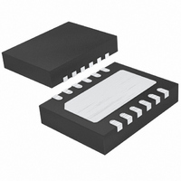
LTC3458EDE#PBF Linear Technology, LTC3458EDE#PBF Datasheet - Page 2

LTC3458EDE#PBF
Manufacturer Part Number
LTC3458EDE#PBF
Description
IC CONV DC/DC SYNC BOOST 12DFN
Manufacturer
Linear Technology
Type
Step-Up (Boost)r
Datasheet
1.LTC3458EDE.pdf
(16 pages)
Specifications of LTC3458EDE#PBF
Internal Switch(s)
Yes
Synchronous Rectifier
Yes
Number Of Outputs
1
Voltage - Output
2 ~ 7.5 V
Current - Output
1.4A
Frequency - Switching
1.5MHz
Voltage - Input
1.5 ~ 6 V
Operating Temperature
-40°C ~ 85°C
Mounting Type
Surface Mount
Package / Case
12-DFN
Dc To Dc Converter Type
Step Up
Pin Count
12
Input Voltage
6V
Output Voltage
2 to 7.5V
Switching Freq
1.15MHz
Output Current
1.6A
Efficiency
93%
Package Type
DFN EP
Output Type
Adjustable
Switching Regulator
Yes
Mounting
Surface Mount
Input Voltage (min)
1.5V
Operating Temp Range
-40C to 85C
Operating Temperature Classification
Industrial
Primary Input Voltage
6V
No. Of Outputs
1
No. Of Pins
12
Operating Temperature Range
-40°C To +85°C
Msl
MSL 1 - Unlimited
Rohs Compliant
Yes
Lead Free Status / RoHS Status
Lead free / RoHS Compliant
Power - Output
-
Lead Free Status / Rohs Status
Compliant
Available stocks
Company
Part Number
Manufacturer
Quantity
Price
ABSOLUTE AXI U RATI GS
LTC3458
(Note 1)
V
BURST, SHDN, V
Operating Temperature Range
Storage Temperature Range ..................–65°C to 125°C
SW Voltage
ORDER INFORMATION
LEAD FREE FINISH
LTC3458EDE#PBF
Consult LTC Marketing for parts specified with wider operating temperature ranges.
Consult LTC for information on nonstandard lead based finish parts.
For more information on lead free part marking, go to:
For more information on tape and reel specifications, go to:
temperature range, otherwise specifications are at T
PARAMETER
Minimum V
Output Voltage Adjust Range
Feedback Voltage
Undervoltage (Exit Burst Mode Operation)
Feedback Input Current
Quiescent Current - Burst Mode Operation
Quiescent Current - Shutdown
Quiescent Current - Active
NMOS Switch Leakage
PMOS Switch Leakage
NMOS Switch On Resistance
PMOS Switch On Resistance
Fixed NMOS Current Limit
Maximum Duty Cycle
Minimum Duty Cycle
Frequency Accuracy
Error Amplifier Transconductance
Error Amplifier Source Current
2
ELECTRICAL CHARACTERISTICS
IN
(Notes 2, 3) .........................................–40°C to 85°C
DC ........................................................... –0.3V to 8V
Pulsed <100ns ...................................... –0.3V to 10V
, SS, SYNC Voltages ................................. –0.3 to 7V
IN
Operating Voltage
OUT
W
TAPE AND REEL
LTC3458EDE#TRPBF
Voltages ....................... –0.3 to 8V
W W
PART MARKING
3458
http://www.linear.com/leadfree/
U
http://www.linear.com/tapeandreel/
A
= 25°C. V
CONDITIONS
T
T
0°C to 85°C, V
–40°C to 0°C
Below Feedback Voltage
V
V
V
V
V
V
V
V
R
V
R
A
A
FB
IN
OUT
IN
OUT
IN
OUT
OUT
IN
ILIM
T
= 0°C to 85°C
= –40°C to 0°C
= 200k
The
Current at 3.3V
Current at 3.3V
Current Switching
= 3.3V, f
= 1.23V
Current at 5V
Current at 0V
= 5V
= 5V
= 124k
●
IN
PACKAGE DESCRIPTION
12-Lead (4mm x 3mm) Plastic DFN
denotes the specifications which apply over the full operating
= 3.3V, V
OSC
OUT
PIN CONFIGURATION
= 1MHz
= 3.3V
OUT
= 5V, R
T
SHDN
SYNC
12-LEAD (4mm × 3mm) PLASTIC DFN
= 200k, unless otherwise noted.
I
SW
EXPOSED PAD IS PGND (PIN 13),
V
LIM
R
IN
MUST BE SOLDERED TO PCB
T
T
JMAX
1
2
3
4
5
6
DE12 PACKAGE
= 125°C, θ
●
●
●
●
●
●
●
TOP VIEW
13
1.21
1.20
0.85
MIN
TEMPERATURE RANGE
–40ºC to 85ºC
2.0
1.4
80
JA
= 45°C/W
12
11
10
9
8
7
V
BURST
SS
GND
COMP
FB
–4%
1.23
0.05
0.05
TYP
OUT
100
1.4
1.4
0.5
0.3
0.4
1.6
15
90
1
5
1
1
1
7
MAX
1.25
1.25
1.15
1.5
1.7
7.5
50
30
10
1
3
3
5
5
0
UNITS
3458fa
μA/V
MHz
mA
nA
μA
μA
μA
μA
μA
μA
μA
%
%
Ω
Ω
V
V
V
V
V
V
A


