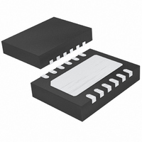
LTC3458EDE#PBF Linear Technology, LTC3458EDE#PBF Datasheet - Page 12

LTC3458EDE#PBF
Manufacturer Part Number
LTC3458EDE#PBF
Description
IC CONV DC/DC SYNC BOOST 12DFN
Manufacturer
Linear Technology
Type
Step-Up (Boost)r
Datasheet
1.LTC3458EDE.pdf
(16 pages)
Specifications of LTC3458EDE#PBF
Internal Switch(s)
Yes
Synchronous Rectifier
Yes
Number Of Outputs
1
Voltage - Output
2 ~ 7.5 V
Current - Output
1.4A
Frequency - Switching
1.5MHz
Voltage - Input
1.5 ~ 6 V
Operating Temperature
-40°C ~ 85°C
Mounting Type
Surface Mount
Package / Case
12-DFN
Dc To Dc Converter Type
Step Up
Pin Count
12
Input Voltage
6V
Output Voltage
2 to 7.5V
Switching Freq
1.15MHz
Output Current
1.6A
Efficiency
93%
Package Type
DFN EP
Output Type
Adjustable
Switching Regulator
Yes
Mounting
Surface Mount
Input Voltage (min)
1.5V
Operating Temp Range
-40C to 85C
Operating Temperature Classification
Industrial
Primary Input Voltage
6V
No. Of Outputs
1
No. Of Pins
12
Operating Temperature Range
-40°C To +85°C
Msl
MSL 1 - Unlimited
Rohs Compliant
Yes
Lead Free Status / RoHS Status
Lead free / RoHS Compliant
Power - Output
-
Lead Free Status / Rohs Status
Compliant
Available stocks
Company
Part Number
Manufacturer
Quantity
Price
LTC3458
APPLICATIO S I FOR ATIO
Input Capacitor Selection
The input filter capacitor reduces peak currents drawn
from the input source and reduces input switching noise.
In most applications >1μF per amp of peak input current
is recommended. See Table 3 for a list of capacitor
manufacturers for input and output capacitor selection.
Table 3. Capacitor Vendor Information
Supplier
AVX
Sanyo
TDK
Murata
Taiyo Yuden
Operating Frequency Selection
There are several considerations in selecting the operating
frequency of the converter. The first is staying clear of
sensitive frequency bands, which cannot tolerate any
spectral noise. For example in products incorporating RF
communications the 455kHz IF frequency is sensitive to
any noise, therefore switching above 600kHz is desired.
Some communications have sensitivity to 1.1MHz and in
that case a 1.5MHz switching converter frequency may be
employed. The second consideration is the physical size of
the converter. As the operating frequency goes up, the
inductor and filter capacitors go down in value and size.
The trade off is in efficiency, since the switching losses due
to gate charge increase proportional with frequency.
Thermal Considerations
For the LTC3458 to deliver its full output power, it is
imperative that a good thermal path be provided to dissi-
pate the heat generated within the package. This can be
accomplished by taking advantage of the large thermal
pad on the underside of the IC. It is recommended that
multiple vias in the printed circuit board be used to
conduct heat away from the IC and into a copper plane with
as much area as possible. If the junction temperature rises
above ~150°C, the part will go into thermal shutdown, and
all switching will stop until the temperature drops.
12
Phone
USA: (814) 237-1431
(803) 448 - 9411
(619) 661 - 6322
(847) 803 - 6100
(800) 831-9172
(408) 573 - 4150
U
U
Website
www.avxcorp.com
www.sanyovideo.com
www.component.tdk.com
www.murata.com
www.t-yuden.com
W
U
Compensating the Feedback Loop
The LTC3458 uses current mode control, with internal
adaptive slope compensation. Current mode control elimi-
nates the 2nd order filter due to the inductor and output
capacitor exhibited in voltage mode controllers, and sim-
plifies the power loop to a single pole filter response. The
product of the modulator control to output DC gain, and
the error amp open-loop gain gives the DC gain of the
system:
The output filter pole is given by:
where C
The output filter zero is given by:
where R
resistance.
A troublesome feature of the boost regulator topology is
the right half plane zero (RHP), and is given by:
At heavy loads this gain increase with phase lag can occur
at a relatively low frequency. The loop gain is typically
G
G
G
f
f
f
FILTER POLE
FILTER ZERO
RHPZ
DC
CONTROL
EA
≈
=
OUT
ESR
=
1000
G
_
_
,
CONTROL
2π •
is the output filter capacitor.
is the output capacitor equivalent series
=
I
2
=
=
OUT
I
OUT
•
π
V
2π
V
IN
IN
•
G
•
•
G
2
V
•
V
,
CURRENT SENSE
OUT
R
OUT
EA
I
OUT
ESR
•
1
•
•
V
V
C
•
L
OUT
REF
C
OUT
_
OUT
•
,
G
,
CURRENT SENSE
=
R
DS ON
1
(
_
)
3458fa


