LTC3458EDE#PBF Linear Technology, LTC3458EDE#PBF Datasheet
LTC3458EDE#PBF
Specifications of LTC3458EDE#PBF
Available stocks


Related parts for LTC3458EDE#PBF


LTC3458EDE#PBF Summary of contents
Page 1
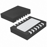
... The LTC3458 is available in a low profile (0.75mm), 3mm × 4mm 12-pin DFN package. , LT, LTC and LTM are registered trademarks of Linear Technology Corporation. All other trademarks are the property of their respective owners. Burst Mode is a registered trademark of Linear Technology Corporation. ...
Page 2
... Pulsed <100ns ...................................... –0.3V to 10V ORDER INFORMATION LEAD FREE FINISH TAPE AND REEL LTC3458EDE#PBF LTC3458EDE#TRPBF Consult LTC Marketing for parts specified with wider operating temperature ranges. Consult LTC for information on nonstandard lead based finish parts. For more information on lead free part marking, go to: ...
Page 3
ELECTRICAL CHARACTERISTICS temperature range, otherwise specifications are at T PARAMETER Error Amplifier Sink Current SYNC Input High SYNC Input Low SHDN Input High SHDN Input Low BURST Mode Peak Current BURST Threshold Voltage Note 1: Stresses beyond those listed under ...
Page 4
LTC3458 W U TYPICAL PERFOR A CE CHARACTERISTICS Frequency Accuracy 1. 200k 1.03 1.01 0.99 0.97 0.95 –45 –30 – TEMPERATURE (°C) 3458 G07 Maximum Load Current 1200 1.8 to 5.5V ...
Page 5
W U TYPICAL PERFOR A CE CHARACTERISTICS Fixed Frequency (FF) Discontinuous Current SW 2V/DIV I L 100mA/DIV V = 3.3V 200ns/DIV OUT L = 10μH Over-Current with 1. 2V/DIV I L 0.5A/DIV V = ...
Page 6
LTC3458 W U TYPICAL PERFOR A CE CHARACTERISTICS Sync Operation at 1.33MHz SW 5V/DIV SYNC 2V/DIV I L 200mA/DIV 500ns/DIV OUT R = 200k OSC Burst Mode Operation 10mA to 50mA Load Step ...
Page 7
CTIO S SW (Pin 1): Switch Pin for Inductor Connection. During discontinuous conduction mode an antiring resistor con- nects reduce noise (Pin 2): Input Supply Pin. Connect this to ...
Page 8
LTC3458 W BLOCK DIAGRA V CC OSC/SYNC SYNC SLOPE 3 MAX R 6 DUTY T I ZERO P-DRIVE PWM AND BURST MODE N-DRIVE DRIVE LOGIC SLEEP CONTROL MODE I FIXED COMP/LIMIT_PEAK FREQUENCY I BURST_PEAK BURST MODE MUX V PGND 9 ...
Page 9
U U APPLICATIO S I FOR ATIO Error Amp. The error amplifier is a transconductance type, with its positive input internally connected to the 1.23V reference, and its negative input connected to FB. A simple compensation network is placed from ...
Page 10
LTC3458 U U APPLICATIO S I FOR ATIO transition occurs using a single resistor. During Burst Mode operation, the oscillator is shut down, since the on time is determined by the time it takes the inductor current to reach a ...
Page 11
U U APPLICATIO S I FOR ATIO COMPONENT SELECTION Inductor Selection The high frequency operation of the LTC3458 allows for the use of small surface mount inductors. Since the internal slope compensation circuit relies on the inductor’s current slope and ...
Page 12
LTC3458 U U APPLICATIO S I FOR ATIO Input Capacitor Selection The input filter capacitor reduces peak currents drawn from the input source and reduces input switching noise. In most applications >1μF per amp of peak input current is recommended. ...
Page 13
U U APPLICATIO S I FOR ATIO rolled off before the RHP zero frequency. The typical error amp compensation is shown in Figure 2. The equations for the loop dynamics are as follows: 1 ≈ f which is close to ...
Page 14
LTC3458 U TYPICAL APPLICATIO S Lithium-Ion to 5V, 500mA at 850kHz WURTH 12μH 774775112 V IN Li-Ion LTC3458 2.2μF 2.5V to 4.2V GND/PGND SHDN ON OFF SYNC R T BURST I LIM 243k 124k Two Cell to 5V WURTH 12μH ...
Page 15
... SHADED AREA IS ONLY A REFERENCE FOR PIN 1 LOCATION ON THE TOP AND BOTTOM OF PACKAGE Information furnished by Linear Technology Corporation is believed to be accurate and reliable. However, no responsibility is assumed for its use. Linear Technology Corporation makes no represen- tation that the interconnection of its circuits as described herein will not infringe on existing patent rights. U DE/UE Package 12-Lead Plastic DFN (4mm × ...
Page 16
... MS10 OUT(MAX 5.25V 12μA, I < 1μA, OUT(MAX 5V 20μA/300μA I < 1μA, OUT(MAX 10V 10μA, ThinSOT OUT(MAX 36V 2mA, I < 1μA, SC70, OUT(MAX 34V 25μA, I < 1μA, OUT(MAX 3458fa LT0807 REV A • PRINTED IN USA © LINEAR TECHNOLOGY CORPORATION 2004 ...