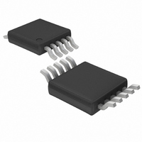
LTC1871EMS-7 Linear Technology, LTC1871EMS-7 Datasheet - Page 26

LTC1871EMS-7
Manufacturer Part Number
LTC1871EMS-7
Description
IC MULTI CONFIG SYNC ADJ 10MSOP
Manufacturer
Linear Technology
Type
Step-Up (Boost), Flyback, Sepicr
Datasheet
1.LTC1871EMS-7.pdf
(32 pages)
Specifications of LTC1871EMS-7
Internal Switch(s)
No
Synchronous Rectifier
No
Number Of Outputs
1
Voltage - Output
1.23 ~ 36 V
Current - Output
50mA
Frequency - Switching
50kHz ~ 1MHz
Voltage - Input
6 ~ 36 V
Operating Temperature
-40°C ~ 85°C
Mounting Type
Surface Mount
Package / Case
10-MSOP, Micro10™, 10-uMAX, 10-uSOP
Lead Free Status / RoHS Status
Contains lead / RoHS non-compliant
Power - Output
-
Available stocks
Company
Part Number
Manufacturer
Quantity
Price
Company:
Part Number:
LTC1871EMS-7
Manufacturer:
LT
Quantity:
10 000
LTC1871-7
APPLICATIONS INFORMATION
rating for the inductor should be checked at the minimum
input voltage (which results in the highest inductor cur-
rent) and maximum output current.
SEPIC Converter: Power MOSFET Selection
Important parameters for the power MOSFET include the
drain-to-source breakdown voltage (BV
voltage (V
to-source voltage, the gate-to-source and gate-to-drain
charges (Q
current (I
(R
The gate drive voltage is set by the 7V INTV
regulator. Consequently, 6V rated threshold MOSFETs are
required in most LTC1871-7 applications.
The maximum voltage that the MOSFET switch must
sustain during the off-time in a SEPIC converter is equal
to the sum of the input and output voltages (V
As a result, careful attention must be paid to the BV
specifi cations for the MOSFETs relative to the maximum
actual switch voltage in the application. Many logic-level
devices are limited to 30V or less. Check the switching
waveforms directly across the drain and source terminals
of the power MOSFET to ensure the V
the maximum rating for the device.
Sense Resistor Selection
During the MOSFET’s on-time, the control circuit limits
the maximum voltage drop across the power MOSFET to
about 150mV (at low duty cycle). The peak inductor cur-
rent is therefore limited to 150mV/R
between the maximum load current, duty cycle and the
sense resistor is:
The V
cycle and is reduced to about 100mV at a duty cycle of
26
TH(JC)
R
SENSE
SENSE(MAX)
and R
D(MAX)
GS(TH)
GS
V
and Q
TH(JA)
SENSE(MAX)
I
), the on-resistance (R
) and the MOSFET’s thermal resistances
O(MAX)
term is typically 150mV at low duty
GD
).
, respectively), the maximum drain
•
1+
1
2
SENSE
•
DS(ON)
DSS
DS
V
V
. The relationship
O
IN(MIN)
remains below
), the threshold
CC
+ V
) versus gate-
low dropout
1
D
O
+ V
+ 1
DSS
IN
).
92% due to slope compensation, as shown in Figure 11.
The constant ‘ χ ’ in the denominator represents the ripple
current in the inductors relative to their maximum cur-
rent. For example, if 30% ripple current is chosen, then
χ = 0.30.
Calculating Power MOSFET Switching and Conduction
Losses and Junction Temperatures
In order to calculate the junction temperature of the
power MOSFET, the power dissipated by the device must
be known. This power dissipation is a function of the
duty cycle, the load current and the junction temperature
itself. As a result, some iterative calculation is normally
required to determine a reasonably accurate value. Since
the controller is using the MOSFET as both a switching
and a sensing element, care should be taken to ensure
that the converter is capable of delivering the required
load current over all operating conditions (load, line and
temperature) and for the worst-case specifi cations for
V
manufacturer’s data sheet.
The power dissipated by the MOSFET in a SEPIC converter
is:
The fi rst term in the equation above represents the I
losses in the device and the second term, the switching
losses. The constant k = 1.7 is an empirical factor inversely
related to the gate drive current and has the dimension
of 1/current.
The ρ
the R
Figure 12 illustrates the variation of normalized R
over temperature for a typical power MOSFET.
SENSE(MAX)
P
+ k • V
FET
DS(ON)
T
term accounts for the temperature coeffi cient of
= I
(
IN
O(MAX)
of the MOSFET, which is typically 0.4%/°C.
and the R
+ V
O
)
2
•
1– D
•I
D
O(MAX)
DS(ON)
2
• R
of the MOSFET listed in the
•
1– D
DS(ON)
D
• C
• D •
RSS
• f
T
DS(ON)
18717fc
2
R


