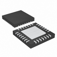
MAX15021ATI+ Maxim Integrated Products, MAX15021ATI+ Datasheet - Page 7

MAX15021ATI+
Manufacturer Part Number
MAX15021ATI+
Description
IC REG SYNC DUAL 28-TQFN-EP
Manufacturer
Maxim Integrated Products
Type
Step-Down (Buck)r
Datasheet
1.MAX15021ATI.pdf
(23 pages)
Specifications of MAX15021ATI+
Internal Switch(s)
Both
Synchronous Rectifier
Yes
Number Of Outputs
2
Voltage - Output
0.6 ~ 5.5 V
Current - Output
2A, 4A
Frequency - Switching
500kHz ~ 4MHz
Voltage - Input
2.5 ~ 5.5 V
Operating Temperature
-40°C ~ 125°C
Mounting Type
Surface Mount
Package / Case
28-TQFN Exposed Pad
Power - Output
2.76W
Topology
Buck
Output Voltage
0.6 V to 5.5 V
Output Current
2 A, 4 A
Input Voltage
2.5 V to 5.5 V
Duty Cycle (max)
100 %
Switching Frequency
500 KHz to 4 MHz
Maximum Operating Temperature
+ 125 C
Mounting Style
SMD/SMT
Minimum Operating Temperature
- 40 C
Operating Supply Voltage
2.5 V to 5.5 V
Lead Free Status / RoHS Status
Lead free / RoHS Compliant
13, 14, 15,
20, 21, 22
Regulator with Tracking/Sequencing Capability
2, 7, 8
PIN
3, 6
4, 5
10
11
12
16
17
18
19
23
24
25
26
27
28
—
1
9
PGND1
DVDD1
COMP1
DVDD2
PGND2
COMP2
NAME
PVIN1
PVIN2
SGND
AVIN
N.C.
EN1
FB1
FB2
EN2
SEL
LX1
LX2
RT
EP
_______________________________________________________________________________________
Track/Sequence Select Input. Connect SEL to ground to configure the device as a sequencer. Connect
SEL to AVIN for tracking with output 1 as the master. Leave SEL unconnected for tracking with output 2
as the master. Use the output with the higher voltage as the master and the output with the lower voltage
as the slave.
Power Ground Connection for Regulator 1. Connect the negative terminals of the input and output filter
capacitor to PGND1. Connect PGND1 externally to SGND at a single point, typically at the negative
terminal of the input capacitor.
Inductor Connection for Regulator 1. LX1 is the drain connection of the internal high-side p-channel
MOSFET and the drain connection of the internal synchronous n-channel MOSFET for regulator 1.
Input Supply Voltage for Regulator 1. Connect to an external voltage source from 2.5V to 5.5V. Bypass
PVIN1 to PGND1 with a 1µF (min) ceramic capacitor.
Switch Driver Supply for Regulator 1. Connect externally to PVIN1.
Enable Input for Regulator 1. When configured as a sequencer, EN1 must exceed 1.225V (typ) for the
PWM controller to begin regulating output 1. When configured as a tracker, connect EN1 to the center
tap of a resistive divider from the regulator 2 output.
Feedback Regulation Point for Regulator 1. Connect FB1 to the center tap of a resistive divider from the
regulator 1 output to SGND to set the output voltage. The FB1 voltage regulates to 0.6V (typ).
Error-Amplifier Output for Regulator 1. Connect COMP1 to the compensation feedback network.
No Connection. Do not connect.
Switch Driver Supply for Regulator 2. Connect externally to PVIN2.
Power Ground Connection for Regulator 2. Connect the negative terminals of the input and output filter
capacitors to PGND2. Connect PGND2 externally to SGND at a single point, typically at the negative
terminal of the input capacitor.
Inductor Connection for Regulator 2. LX2 is the drain connection of the internal high-side p-channel
MOSFET and the drain connection of the internal synchronous n-channel MOSFET for regulator 2.
Input Supply Voltage for Regulator 2. Connect to an external voltage source from 2.5V to 5.5V. Bypass
PVIN2 to PGND2 with a 1µF (min) ceramic capacitor.
Error-Amplifier Output for Regulator 2. Connect COMP2 to the compensation feedback network.
Feedback Regulation Point for Regulator 2. Connect to the center tap of a resistive divider from the
regulator 2 output to SGND to set the output voltage. The FB2 voltage regulates to 0.6V (typ).
Enable Input for Regulator 2. When configured as a sequencer, EN2 must exceed 1.225V (typ) for the
PWM controller to begin regulating output 2. When configured as a tracker, connect EN2 to the center
tap of a resistive divider from the regulator 1 output.
Signal Ground. Connect SGND to PGND_ at a single point, typically near negative terminal of the input
bypass capacitor.
Input Voltage. Bypass AVIN to SGND with a 100nF (min) ceramic capacitor.
Oscillator Timing Resistor Connection. Connect a 4.2kΩ to 33kΩ resistor from RT to SGND to program
the switching frequency from 500kHz to 4MHz.
Exposed Pad. Connect EP to a large copper plane at SGND potential to improve thermal dissipation. Do
not use as the main SGND connection.
Dual, 4A/2A, 4MHz, Step-Down DC-DC
FUNCTION
Pin Description
7


