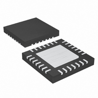
MAX15021ATI+ Maxim Integrated Products, MAX15021ATI+ Datasheet - Page 13

MAX15021ATI+
Manufacturer Part Number
MAX15021ATI+
Description
IC REG SYNC DUAL 28-TQFN-EP
Manufacturer
Maxim Integrated Products
Type
Step-Down (Buck)r
Datasheet
1.MAX15021ATI.pdf
(23 pages)
Specifications of MAX15021ATI+
Internal Switch(s)
Both
Synchronous Rectifier
Yes
Number Of Outputs
2
Voltage - Output
0.6 ~ 5.5 V
Current - Output
2A, 4A
Frequency - Switching
500kHz ~ 4MHz
Voltage - Input
2.5 ~ 5.5 V
Operating Temperature
-40°C ~ 125°C
Mounting Type
Surface Mount
Package / Case
28-TQFN Exposed Pad
Power - Output
2.76W
Topology
Buck
Output Voltage
0.6 V to 5.5 V
Output Current
2 A, 4 A
Input Voltage
2.5 V to 5.5 V
Duty Cycle (max)
100 %
Switching Frequency
500 KHz to 4 MHz
Maximum Operating Temperature
+ 125 C
Mounting Style
SMD/SMT
Minimum Operating Temperature
- 40 C
Operating Supply Voltage
2.5 V to 5.5 V
Lead Free Status / RoHS Status
Lead free / RoHS Compliant
Although the MAX15021’s regulators can operate from
input supplies ranging from 2.5V to 5.5V, the input-volt-
age range can be effectively limited by the
MAX15021’s duty-cycle limitations for a given output
voltage (V
(V
lable minimum on-time (t
where t
The minimum input voltage (V
tively limited by the maximum controllable duty cycle
and is calculated using the following equation:
where V
t
Three key inductor parameters must be specified for
operation with the MAX15021: inductance value (L),
peak inductor current (I
current (I
function of operating frequency, input-to-output voltage
differential, and the peak-to-peak inductor current
(∆I
lower inductance minimizes size and cost and
improves large-signal and transient response.
However, efficiency is reduced due to higher peak cur-
rents and higher peak-to-peak output-voltage ripple for
the same output capacitor. A higher inductance
increases efficiency by reducing the ripple current;
however, resistive losses due to extra wire turns can
exceed the benefit gained from lower ripple current lev-
els especially when the inductance is increased without
also allowing for larger inductor dimensions. Choose
the inductor’s peak-to-peak current, ∆I
of 20% to 50% of the full load current; as a rule of
thumb 30% is typical.
Calculate the inductance, L, using the following equation:
OFF(MIN)
Regulator with Tracking/Sequencing Capability
PVIN_MAX
P-P
). Higher ∆I
V
PVIN_MIN
L H
ON(MIN)
V
[
PVIN_MAX
µ
OUT_
SAT
is the 0.06µs (typ) controllable off-time.
) can be effectively limited by the control-
]
OUT_
=
). The minimum required inductance is a
V
is the regulator output voltage and
V
is 0.06µs (typ).
OUT_
[V]
PVIN_
Effective Input-Voltage Range
P-P
). The maximum input voltage
______________________________________________________________________________________
[V]
≥
allows for a lower inductor value. A
1 (t
[V] (V
≤
−
[V] f
t
ON(MIN)
×
ON(MIN)
PEAK
OFF(MIN)
×
Dual, 4A/2A, 4MHz, Step-Down DC-DC
SW
PVIN_
), and inductor saturation
[MHz]
V
PVIN_MIN
V
Inductor Selection
OUT_
OUT_
):
[ s] f
µ
[V] V
[ s] f
µ
×
−
×
[V]
[V]
×
SW
∆
P-P,
OUT_
SW
) can be effec-
I
P P
[MHz]
−
[MHz])
in the range
[V])
[ ]
A
where V
regulator output voltage, and f
quency. Use typical values for V
that efficiency is optimum for typical conditions. The
switching frequency (f
500kHz and 4MHz (see the Oscillator section).
The peak-to-peak inductor current (∆I
reflects the peak-to-peak output ripple, is largest at the
maximum input voltage. See the Output-Capacitor
Selection section to verify that the worst-case output
current ripple is acceptable.
Select an inductor with a saturation current, I
er than the maximum peak current to avoid runaway
current during continuous output short-circuit condi-
tions. Also, confirm that the inductor’s thermal perfor-
mances and projected temperature rise above ambient
does not exceed its thermal capacity. Many inductor
manufacturers provide bias/load current versus tem-
perature rise performance curves (or similar) to obtain
this information.
The discontinuous input current of the buck converter
causes large input ripple currents and therefore, the
input capacitor must be carefully chosen to withstand
the input ripple current and keep the input-voltage rip-
ple within design requirements.
The input-voltage ripple is comprised of ∆V
the capacitor discharge) and ∆V
of the input capacitor). The total voltage ripple is the
sum of ∆V
on-cycle. Calculate the required input capacitance and
ESR for a specified ripple using the following equations:
I
peak-to-peak inductor current, and V
supply voltage, V
and f
LOAD(MAX)
SW
C
∆
PVIN_
I
is the switching frequency.
PVIN_
P P
ESR
Q
−
is the maximum output current, ∆I
[A]
and ∆V
[
[
is the input supply voltage, V
m
µ
F
=
Ω
]
OUT_
]
(
=
V
=
V
PVIN_
ESR
I
PVIN_
LOAD(MAX)
⎛
⎜
⎝
Input-Capacitor Selection
I
LOAD(MAX)
SW
is the regulator output voltage,
which peaks at the end of the
∆
[V] f
−
) is programmable between
V [V] f
V
Q
∆
OUT_
×
V
ESR
SW
SW
ESR
[A]
×
+
)
PVIN_
[mV]
[MHz] L
[V] V
SW
is the switching fre-
×
(caused by the ESR
∆
⎛
⎜
⎝
I
P P
PVIN_
[MHz]
×
V
V
2
−
PVIN_
OUT_
and V
×
OUT_
⎞
⎟
⎠
Q
[A]
P-P
[
OUT_
is the input
µ
(caused by
[V]
[V]
SAT
H
[V]
P-P
), which
]
OUT_
⎞
⎟
⎠
, high-
is the
is the
13
so


