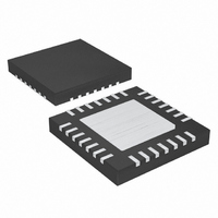
MAX15021ATI+ Maxim Integrated Products, MAX15021ATI+ Datasheet - Page 17

MAX15021ATI+
Manufacturer Part Number
MAX15021ATI+
Description
IC REG SYNC DUAL 28-TQFN-EP
Manufacturer
Maxim Integrated Products
Type
Step-Down (Buck)r
Datasheet
1.MAX15021ATI.pdf
(23 pages)
Specifications of MAX15021ATI+
Internal Switch(s)
Both
Synchronous Rectifier
Yes
Number Of Outputs
2
Voltage - Output
0.6 ~ 5.5 V
Current - Output
2A, 4A
Frequency - Switching
500kHz ~ 4MHz
Voltage - Input
2.5 ~ 5.5 V
Operating Temperature
-40°C ~ 125°C
Mounting Type
Surface Mount
Package / Case
28-TQFN Exposed Pad
Power - Output
2.76W
Topology
Buck
Output Voltage
0.6 V to 5.5 V
Output Current
2 A, 4 A
Input Voltage
2.5 V to 5.5 V
Duty Cycle (max)
100 %
Switching Frequency
500 KHz to 4 MHz
Maximum Operating Temperature
+ 125 C
Mounting Style
SMD/SMT
Minimum Operating Temperature
- 40 C
Operating Supply Voltage
2.5 V to 5.5 V
Lead Free Status / RoHS Status
Lead free / RoHS Compliant
When the f
tion network provides the necessary closed-loop com-
pensated response. The Type II compensation network
provides a midband compensating zero and a high-fre-
quency pole (see Figures 5a and 5b).
R
R
Use the following procedure to calculate the compen-
sation network components.
Calculate the f
where C
is the series resistance of C
Capacitor Selection section for more information on cal-
culating C
Set the compensator’s leading zero, f
filter’s resonant double-pole frequency from:
Set the compensator’s high-frequency pole, f
below one-half the switching frequency, f
To maximize the compensator’s phase lead, set the
desired crossover frequency, f
ric mean of the compensator’s leading zero, f
high-frequency pole, f
Select the feedback resistor, R
to 30kΩ.
Calculate the gain of the modulator (Gain
prised of the regulator’s pulse-width modulator, LC filter,
feedback divider, and associated circuitry—at the desired
crossover frequency, f
where V
L is the value of the regulator inductor, ESR is the
F
Gain
F
Regulator with Tracking/Sequencing Capability
C
C
CF
F
MOD
provides the midband zero f
provides the high-frequency pole, f
Type II: Compensation when f
FB
OUT
OUT
CO
=
is the 0.6V (typ) FB_ input-voltage set-point,
4(V/V)
is the regulator output capacitor and ESR
is greater than f
ESR
and ESR.
f
ESR
f
LC
______________________________________________________________________________________
and LC double pole, f
×
f
(
CO
CO
=
≈
2
P1
π
f
2
2
P1
f
, using the following equation:
, as follows:
×
Z1
=
π
π
f
Dual, 4A/2A, 4MHz, Step-Down DC-DC
×
CO
×
≤
ESR [m ]
≤
ESR C
f
Z1
f
f
SW
L C
[kHz]
LC
2
ESR
1
×
CO
×
1
F
OUT
×
f
, in the range of 3.3kΩ
P1
, equal to the geomet-
, a Type II compensa-
OUT
Ω
OUT
×
. See the Output-
L[ H]
Z1
µ
CO
MID,ZERO
, at or below the
LC
SW
)
:
MOD
> f
×
:
HIGH,POLE
V
ZERO,ESR
OUT_
V
P1
)—com-
FB
Z1
, at or
, and
, and
[V]
[V]
.
series resistance of the output capacitor, and V
the desired output voltage.
The gain of the error amplifier (Gain
frequencies is:
The total loop gain is the product of the modulator gain
and the error amplifier gain at f
equal to 1 as follows:
So:
Figure 5a. Type II Compensation Network
Figure 5b. Type II Compensation Network Response
GAIN
20 log
(dB)
×
R
R
(AT ORIGIN)
1ST ASYMPTOTE
1ST POLE
1
2
V
OUT_
(ωR
10
1
C
⎡
⎢
⎣
F
)
R
R
-1
R
R
F
1
F
1
⎤
⎥
⎦
Gain
+
1ST ZERO
×
(R
Gain
20 log
V
F
2
C
FB_
REF
π
F
MOD
)
×
-1
×
4 ESR x V
E/A
f
×
CO
2ND ASYMPTOTE
10
x Gain
=
R
×
C
(R
⎡
⎢
⎢
⎣
F
CF
R [k ]
L x V
R [k ]
2
F
R
F
1
π
1
)
×
4 ESR x V
-1
E/A
CO
f
×
FB
CO
OUT_
Ω
Ω
C
F
E/A
= 1
×
and should be set
3RD ASYMPTOTE
L x V
2ND POLE
(ωR
(R
) in the midband
F
=
C
F
FB
CF
1
C
OUT_
CF
)
-1
)
-1
⎤
⎥
⎥
⎦
COMP_
ω (rad/sec)
=
OUT_
0dB
17
is


