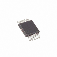
MAX1957EUB+ Maxim Integrated Products, MAX1957EUB+ Datasheet - Page 2

MAX1957EUB+
Manufacturer Part Number
MAX1957EUB+
Description
IC CNTRLR PWM BUCK 10-UMAX
Manufacturer
Maxim Integrated Products
Type
Step-Down (Buck)r
Datasheet
1.MAX1954EUB.pdf
(22 pages)
Specifications of MAX1957EUB+
Internal Switch(s)
No
Synchronous Rectifier
Yes
Number Of Outputs
1
Voltage - Output
0.4 ~ 4.73 V
Current - Output
3A
Frequency - Switching
300kHz
Voltage - Input
3 ~ 5.5 V
Operating Temperature
-40°C ~ 85°C
Mounting Type
Surface Mount
Package / Case
10-MSOP, Micro10™, 10-uMAX, 10-uSOP
Power - Output
444mW
Duty Cycle (max)
89 %
Output Voltage
0.4 V to 4.73 V
Output Current
3000 mA
Mounting Style
SMD/SMT
Switching Frequency
300 KHz
Maximum Operating Temperature
+ 85 C
Minimum Operating Temperature
- 40 C
Synchronous Pin
No
Topology
Boost, Buck
Lead Free Status / RoHS Status
Lead free / RoHS Compliant
ABSOLUTE MAXIMUM RATINGS
IN, FB to GND...........................................................-0.3V to +6V
LX to BST..................................................................-6V to +0.3V
BST to GND ............................................................-0.3V to +20V
DH to LX ....................................................-0.3V to (V
DL, COMP to GND.......................................-0.3V to (V
HSD, ILIM, REFIN to GND ........................................-0.3V to 14V
PGND to GND .......................................................-0.3V to +0.3V
I
Low-Cost, High-Frequency, Current-Mode PWM
Buck Controller
Stresses beyond those listed under “Absolute Maximum Ratings” may cause permanent damage to the device. These are stress ratings only, and functional
operation of the device at these or any other conditions beyond those indicated in the operational sections of the specifications is not implied. Exposure to
absolute maximum rating conditions for extended periods may affect device reliability.
ELECTRICAL CHARACTERISTICS
(V
2
DH
Operating Input Voltage Range
HSD Voltage Range
Quiescent Supply Current
Standby Supply Current (MAX1953/ MAX1957) V
Standby Supply Current (MAX1954)
Undervoltage Lockout Trip Level
Output Voltage Adjust Range (V
ERROR AMPLIFIER
FB Regulation Voltage
Transconductance
FB Input Leakage Current
REFIN Input Bias Current
FB Input Common-Mode Range
REFIN Input Common-Mode Range
Current-Sense Amplifier Voltage Gain Low
Current-Sense Amplifier Voltage Gain
IN
, I
_______________________________________________________________________________________
= 5V, V
DL
................................................................±100mA (RMS)
BST
- V
PARAMETER
LX
= 5V, T
A
= -40°C to +85°C, unless otherwise noted. Typical values are at T
OUT
)
MAX1954 only (Note 2)
V
V
COMP = GND
Rising and falling V
T
T
MAX1957 only
V
V
MAX1957 only
ILIM = GND (MAX1953 only)
V
MAX1954/MAX1957
FB
IN
IN
A
A
FB
REFIN
ILIM
BST
= 0 C to +85 C (MAX1953/MAX1954)
= -40 C to +85 C (MAX1953/MAX1954)
IN
= V
= V
= 1.5V, no switching
= 0.9V
= V
+ 0.3V)
+ 0.3V)
BST
BST
= 0.8V, MAX1957 only
IN
= 5.5V, COMP = GND
= 5.5V, V
or ILIM = open (MAX1953 only)
CONDITIONS
IN
Continuous Power Dissipation (T
Operating Temperature Range ...........................-40°C to +85°C
Junction Temperature ......................................................+150°C
Storage Temperature Range .............................-65°C to +150°C
Lead Temperature (soldering, 10s) .................................+300°C
HSD
, 3% hysteresis
(derate 5.6mW/°C above +70°C) ..................................444mW
= 13.2V,
A
V
- 8mV
0.788
0.776
2.50
5.67
3.15
MIN
REFIN
-0.1
-0.1
= +25°C.) (Note 1)
3.0
3.0
0.8
70
A
= +70°C)
V
TYP
2.78
REFIN
220
220
110
0.8
0.8
6.3
3.5
1
5
5
V
+ 8mV
0.86 x
0.812
0.812
MAX
13.2
2.95
6.93
3.85
REFIN
350
350
160
500
500
V
5.5
1.5
1.5
2
IN
UNITS
mA
V/V
V/V
µA
µA
µS
nA
nA
V
V
V
V
V
V
V


