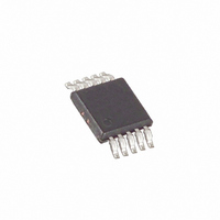
MAX1957EUB+ Maxim Integrated Products, MAX1957EUB+ Datasheet - Page 19

MAX1957EUB+
Manufacturer Part Number
MAX1957EUB+
Description
IC CNTRLR PWM BUCK 10-UMAX
Manufacturer
Maxim Integrated Products
Type
Step-Down (Buck)r
Datasheet
1.MAX1954EUB.pdf
(22 pages)
Specifications of MAX1957EUB+
Internal Switch(s)
No
Synchronous Rectifier
Yes
Number Of Outputs
1
Voltage - Output
0.4 ~ 4.73 V
Current - Output
3A
Frequency - Switching
300kHz
Voltage - Input
3 ~ 5.5 V
Operating Temperature
-40°C ~ 85°C
Mounting Type
Surface Mount
Package / Case
10-MSOP, Micro10™, 10-uMAX, 10-uSOP
Power - Output
444mW
Duty Cycle (max)
89 %
Output Voltage
0.4 V to 4.73 V
Output Current
3000 mA
Mounting Style
SMD/SMT
Switching Frequency
300 KHz
Maximum Operating Temperature
+ 85 C
Minimum Operating Temperature
- 40 C
Synchronous Pin
No
Topology
Boost, Buck
Lead Free Status / RoHS Status
Lead free / RoHS Compliant
so the loop-gain equation at the crossover frequency is:
For the case where f
then R
where g
The error amplifier compensation zero formed by R
and C
C
As the load current decreases, the modulator pole also
decreases. However, the modulator gain increases
accordingly, and the crossover frequency remains the
same. For the case where f
another compensation capacitor C
to cancel the ESR zero at f
Figure 6 illustrates a numerical example that calculates
R
Figure 1 (MAX1953).
Table 2. Suggested Manufacturers
C
Central Semiconductor
Coilcraft
Fairchild
Kemet
Panasonic
Taiyo Yuden
Toko
C
Low-Cost, High-Frequency, Current-Mode PWM
is calculated by:
and
G
and C
MOD f
MANUFACTURER
C
C
mEA
C
is calculated as:
should be set at the modulator pole f
( )
C
C
G
C
R
EA f
values for the typical application circuit of
= 110µS.
C
I
I
( )
OUT MAX
OUT MAX
C
g
G
V
V
C
mc
g
______________________________________________________________________________________
OUT
OUT
EA f
f
(
(
mEA
zESR
( )
G
C
2
MOD f
R
)
)
R
LOAD
is greater than f
LOAD
zESR
V
( )
g
V
FB
(
(
R
f
f
zESR
C
OUT
S
S
mEA
C
. C
1
(
f
f
(
L
L
f
s
G
f
is less than f
is calculated by:
f
V
s
)
)
from COMP to GND
zESR
V
MOD f
OUT
FB
COMPONENT
R
C
Capacitors
Capacitors
Capacitors
MOSFETs
L
Inductors
Inductors
L
C
)
( )
)
Diode
c
R
OUT
:
C
C
1
f
pMOD
f
C
C
pMOD
, add
C
.
See Table 2 for suggested manufacturers of the com-
ponents used with the MAX1953/MAX1954/MAX1957.
Careful PC board layout is critical to achieve low
switching losses and clean, stable operation. The
switching power stage requires particular attention.
Follow these guidelines for good PC board layout:
1) Place decoupling capacitors as close to IC pins as
2) Input and output capacitors are connected to the
3) Keep the high current paths as short as possible.
4) Connect the drain leads of the power MOSFET to a
5) Ensure all feedback connections are short and
6) Route high-speed switching nodes away from sensi-
7) Place the high-side MOSFET as close as possible to
8) Use very short, wide traces (50mils to 100mils wide
TRANSISTOR COUNT: 2930
PROCESS: BiCMOS
possible. Keep separate power ground plane (con-
nected to pin 7) and signal ground plane (connect-
ed to pin 4).
power ground plane; all other capacitors are con-
nected to the signal ground plane.
large copper area to help cool the device. Refer to
the power MOSFET data sheet for recommended
copper area.
direct. Place the feedback resistors as close to the
IC as possible.
tive analog areas (FB, COMP).
the controller and connect IN (MAX1953/MAX1957)
or HSD (MAX1954) and LX to the MOSFET.
if the MOSFET is 1in from the device).
631-435-1110
800-322-2645
800-341-0392
864-963-6300
714-373-7366
408-573-4150
800-745-8656
PHONE
Applications Information
Buck Controller
PC Board Layout Guidelines
www.centralsemi.com
www.coilcraft.com
www.fairchildsemi.com
www.kemet.com
www.panasonic.com
www.t-yuden.com
www.toko.com
Chip Information
WEBSITE
19


