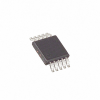
MAX1957EUB+ Maxim Integrated Products, MAX1957EUB+ Datasheet - Page 14

MAX1957EUB+
Manufacturer Part Number
MAX1957EUB+
Description
IC CNTRLR PWM BUCK 10-UMAX
Manufacturer
Maxim Integrated Products
Type
Step-Down (Buck)r
Datasheet
1.MAX1954EUB.pdf
(22 pages)
Specifications of MAX1957EUB+
Internal Switch(s)
No
Synchronous Rectifier
Yes
Number Of Outputs
1
Voltage - Output
0.4 ~ 4.73 V
Current - Output
3A
Frequency - Switching
300kHz
Voltage - Input
3 ~ 5.5 V
Operating Temperature
-40°C ~ 85°C
Mounting Type
Surface Mount
Package / Case
10-MSOP, Micro10™, 10-uMAX, 10-uSOP
Power - Output
444mW
Duty Cycle (max)
89 %
Output Voltage
0.4 V to 4.73 V
Output Current
3000 mA
Mounting Style
SMD/SMT
Switching Frequency
300 KHz
Maximum Operating Temperature
+ 85 C
Minimum Operating Temperature
- 40 C
Synchronous Pin
No
Topology
Boost, Buck
Lead Free Status / RoHS Status
Lead free / RoHS Compliant
Low-Cost, High-Frequency, Current-Mode PWM
Buck Controller
The MAX1953/MAX1954/MAX1957s’ current-sense cir-
cuit amplifies (A
(the high-side MOSFET’s on-resistance (R
plied by the inductor current). This amplified current-
sense signal and the internal-slope compensation
signal are summed (V
PWM comparator’s inverting input. The PWM compara-
tor shuts off the high-side MOSFET when V
exceeds the integrated feedback voltage (V
The current-limit circuit employs a lossless current-limit-
ing algorithm that uses the low-side and high-side
MOSFETs’ on-resistances as the sensing elements. The
voltage across the high-side MOSFET is monitored for
current-mode feedback, as well as current limit. This
signal is amplified by the current-sense amplifier and is
compared with a current-sense voltage. If the current-
sense signal is larger than the set current-limit voltage,
the high-side MOSFET turns off. Once the high-side
MOSFET turns off, the low-side MOSFET is monitored
for current limit. If the voltage across the low-side MOS-
FET (R
circuit current limit, the high-side MOSFET turns on
normally. In this condition, the output drops smoothly
out of regulation. If the voltage across the low-side
MOSFET exceeds the short-circuit current-limit thresh-
old at the beginning of each new oscillator cycle, the
MAX1953/MAX1954/MAX1957 do not turn on the high-
side MOSFET.
In the case where the output is shorted, the low-side
MOSFET is monitored for current limit. The low-side
MOSFET is held on to let the current in the inductor
ramp down. Once the voltage across the low-side
MOSFET drops below the short-circuit current-limit
threshold, the high-side MOSFET is pulsed. Under this
condition, the frequency of the MAX1953/MAX1954/
MAX1957 appears to decrease because the on-time of
the low-side MOSFET extends beyond a clock cycle.
The actual peak output current is greater than the
short-circuit current-limit threshold by an amount equal
to the inductor ripple current. Therefore, the exact cur-
rent-limit characteristic and maximum load capability
are a function of the low-side MOSFET on-resistance,
inductor value, input voltage, and output voltage.
The short-circuit current-limit threshold is preset for the
MAX1954/MAX1957 at 210mV. The MAX1953, however,
has three options for the current-limit threshold: con-
nect ILIM to IN for a 320mV threshold, connect ILIM to
GND for 105mV, or leave floating for 210mV.
14
______________________________________________________________________________________
DS(ON)
✕
I
V
INDUCTOR
= 3.5 typ) the current-sense voltage
SUM
Current-Sense Amplifier
) does not exceed the short-
) together and fed into the
Current-Limit Circuit
DS(ON)
COMP
) multi-
).
SUM
Synchronous rectification reduces conduction losses in
the rectifier by replacing the normal Schottky catch
diode with a low-resistance MOSFET switch. The
MAX1953/MAX1954/MAX1957 use the synchronous
rectifier to ensure proper startup of the boost gate-
driver circuit and to provide the current-limit signal. The
DL low-side waveform is always the complement of the
DH high-side drive waveform. A dead-time circuit moni-
tors the DL output and prevents the high-side MOSFET
from turning on until DL is fully off, thus preventing
cross-conduction or shoot-through. In order for the
dead-time circuit to work properly, there must be a low-
resistance, low-inductance path from the DL driver to
the MOSFET gate. Otherwise, the sense circuitry in the
MAX1953/MAX1954/MAX1957 can interpret the MOS-
FET gate as OFF when gate charge actually remains.
The dead time at the other edge (DH turning off) is
determined through gate sensing as well.
Gate-drive voltage for the high-side switch is generated
by a flying capacitor boost circuit (Figure 5). The
capacitor between BST and LX is charged from the V
supply up to V
side MOSFET is on. When the low-side MOSFET is
switched off, the stored voltage of the capacitor is
stacked above LX to provide the necessary turn-on
voltage (V
then closes an internal switch between BST and DH to
turn the high-side MOSFET on.
If the supply voltage at IN drops below 2.75V, the
MAX1953/MAX1954/MAX1957 assume that the supply
voltage is too low to make valid decisions, so the UVLO
circuitry inhibits switching and forces the DL and DH
gate drivers low. After the voltage at IN rises above
2.8V, the controller goes into the startup sequence and
resumes normal operation.
The MAX1953/MAX1954/MAX1957 start switching when
the voltage at IN rises above the UVLO threshold.
However, the controller is not enabled unless all four of
the following conditions are met:
• V
• The internal reference voltage exceeds 92% of its
• The internal bias circuitry powers up.
• The thermal overload limit is not exceeded.
nominal value (V
IN
exceeds the 2.8V UVLO threshold.
GS
High-Side Gate-Drive Supply (BST)
Synchronous Rectifier Driver (DL)
) for the high-side MOSFET. The controller
IN
, minus the diode drop while the low-
REF
> 1 V).
Undervoltage Lockout
Startup
IN


