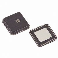
ADP1829ACPZ-R7 Analog Devices Inc, ADP1829ACPZ-R7 Datasheet - Page 4

ADP1829ACPZ-R7
Manufacturer Part Number
ADP1829ACPZ-R7
Description
IC BUCK SYNC ADJ 100uA 32LFCSP
Manufacturer
Analog Devices Inc
Type
Step-Down (Buck)r
Datasheet
1.ADP1829ACPZ-R7.pdf
(32 pages)
Specifications of ADP1829ACPZ-R7
Internal Switch(s)
No
Synchronous Rectifier
Yes
Number Of Outputs
2
Voltage - Output
0.6 ~ 15 V
Current - Output
100µA
Frequency - Switching
300kHz, 600kHz
Voltage - Input
3 ~ 18 V
Operating Temperature
-40°C ~ 125°C
Mounting Type
Surface Mount
Package / Case
32-LFCSP
Power - Output
1W
Primary Input Voltage
20V
No. Of Outputs
2
Output Voltage
17V
No. Of Pins
32
Operating Temperature Range
-40°C To +85°C
Msl
MSL 3 - 168 Hours
Frequency Max
1MHz
Termination Type
SMD
Lead Free Status / RoHS Status
Lead free / RoHS Compliant
For Use With
ADP1829-EVALZ - BOARD EVALUATION ADP1829
Lead Free Status / RoHS Status
Lead free / RoHS Compliant, Lead free / RoHS Compliant
Other names
ADP1829ACPZ-R7TR
ADP1829
Parameter
OSCILLATOR
CURRENT SENSE
GATE DRIVERS
LOGIC THRESHOLDS
THERMAL SHUTDOWN
POWER GOOD
1
2
3
Not recommended to use the LDO in dropout when V
SYNC input frequency is 2× single-channel switching frequency. The SYNC frequency is divided by 2 and the separate phases were used to clock the controllers.
Guaranteed by design and not subject to production test.
Oscillator Frequency
SYNC Synchronization Range
SYNC Minimum Input Pulse Width
CSL1, CSL2 Threshold Voltage
CSL1, CSL2 Output Current
Current Sense Blanking Period
DH1, DH2 Rise Time
DH1, DH2 Fall Time
DL1, DL2 Rise Time
DL1, DL2 Fall Time
DH to DL, DL to DH Dead Time
SYNC, FREQ, LDOSD Input High Voltage
SYNC, FREQ, LDOSD Input Low Voltage
SYNC, FREQ Input Leakage Current
LDOSD Pull-Down Resistance
EN1, EN2 Input High Voltage
EN1, EN2 Input Low Voltage
EN1, EN2 Current Source
EN1, EN2 Input Impedance to 5 V Zener
Thermal Shutdown Threshold
Thermal Shutdown Hysteresis
FB1, UV2 Overvoltage Threshold
FB1, UV2 Overvoltage Hysteresis
FB1, UV2 Undervoltage Threshold
FB1, UV2 Undervoltage Hysteresis
POK1, POK2 Propagation Delay
POK1, POK2 Off Leakage Current
POK1, POK2 Output Low Voltage
UV2 Input Bias Current
2
3
3
IN
Conditions
SYNC = FREQ = GND (f
SYNC = GND, FREQ = VREG (f
FREQ = GND, SYNC = 600 kHz to 1.2 MHz (f
FREQ = VREG, SYNC = 1.2 MHz to 2 MHz (f
CSL1, CSL2 = PGND
C
C
C
C
SYNC, FREQ = 0 V to 5.5 V
IN = 3.0 V to 20 V
IN = 3.0 V to 20 V
EN1, EN2 = 0 V to 3.0 V
EN1, EN2 = 5.5 V to 20 V
V
I
Relative to PGND
V
V
POK1,
< 5.5 V because of the dropout voltage. Connect IN to VREG when V
DH
DH
DL
DL
FB1,
FB1,
POK1,
= 3 nF
= 3 nF
= 3 nF, V
= 3 nF, V
V
V
I
POK2
V
UV2
UV2
POK2
rising
rising
= 10 mA
= 5.5 V
BST
BST
− V
− V
Rev. B | Page 4 of 32
SW
SW
= 5 V
= 5 V
SW
= f
OSC
SW
)
= f
OSC
)
SW
SW
= f
= f
SYNC
SYNC
/2)
/2)
IN
< 5.5 V.
Min
240
480
300
600
−30
44
2.2
2.0
−0.3
Typ
300
600
0
50
100
15
10
15
10
40
100
−0.6
100
145
15
750
50
550
50
8
150
10
Max
370
720
600
1000
200
+30
56
0.4
1
0.8
−1.5
1
500
100
Unit
kHz
kHz
kHz
kHz
ns
mV
μA
ns
ns
ns
ns
ns
ns
V
V
μA
kΩ
V
V
μA
kΩ
°C
°C
mV
mV
mV
mV
μs
μA
mV
nA


