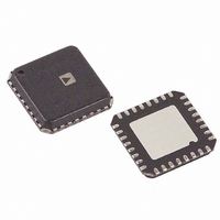
ADP1829ACPZ-R7 Analog Devices Inc, ADP1829ACPZ-R7 Datasheet - Page 18

ADP1829ACPZ-R7
Manufacturer Part Number
ADP1829ACPZ-R7
Description
IC BUCK SYNC ADJ 100uA 32LFCSP
Manufacturer
Analog Devices Inc
Type
Step-Down (Buck)r
Datasheet
1.ADP1829ACPZ-R7.pdf
(32 pages)
Specifications of ADP1829ACPZ-R7
Internal Switch(s)
No
Synchronous Rectifier
Yes
Number Of Outputs
2
Voltage - Output
0.6 ~ 15 V
Current - Output
100µA
Frequency - Switching
300kHz, 600kHz
Voltage - Input
3 ~ 18 V
Operating Temperature
-40°C ~ 125°C
Mounting Type
Surface Mount
Package / Case
32-LFCSP
Power - Output
1W
Primary Input Voltage
20V
No. Of Outputs
2
Output Voltage
17V
No. Of Pins
32
Operating Temperature Range
-40°C To +85°C
Msl
MSL 3 - 168 Hours
Frequency Max
1MHz
Termination Type
SMD
Lead Free Status / RoHS Status
Lead free / RoHS Compliant
For Use With
ADP1829-EVALZ - BOARD EVALUATION ADP1829
Lead Free Status / RoHS Status
Lead free / RoHS Compliant, Lead free / RoHS Compliant
Other names
ADP1829ACPZ-R7TR
ADP1829
SETTING THE CURRENT LIMIT
The current-limit comparator measures the voltage across the
low-side MOSFET to determine the load current.
The current limit is set through the current-limit resistor, R
The current sense pins, CSL1 and CSL2, source 50 μA through
their respective R
by the 50 μA CSL current. When the drop across the low-side
MOSFET R
ADP1829 flags a current-limit event.
Because the CSL current and the MOSFET R
process and temperature, the minimum current limit should be
set to ensure that the system can handle the maximum desired
load current. To do this, use the peak current in the inductor,
which is the desired current-limit level plus the ripple current,
the maximum R
temperature, and the minimum CSL current.
where I
In addition, the ADP1829 offers a technique for implementing
a current-limit foldback in the event of a short circuit with the
use of an additional resistor, as shown in Figure 25. Resistor R
is largely responsible for setting the foldback current limit during
a short circuit, and R
normal current limit. R
sense resistors can be calculated by
where:
I
I
and is also used in Equation 15.
PKFOLDBACK
LPK
is the peak inductor current limit during normal operation
R
R
R
CL
LO
HI
LPK
=
=
=
is the desired short circuit peak inductor current limit.
is the peak inductor current.
DSON
I
I
I
LPK
PKFOLDBACK
LPK
is equal to or greater than this offset voltage, the
DSON
CL
R
44
R
. This creates an offset voltage of R
DSON
DSON
μA
of the MOSFET at its highest expected
44
HI
R
V
LO
is mainly responsible for setting up the
LO
( MAX
μA
(
R
OUT
MAX
DSON
is lower than R
)
)
(MAX
−
44
)
μA
HI
. These current-limit
DSON
vary over
CL
multiplied
CL
(15)
(16)
(17)
Rev. B | Page 18 of 32
.
LO
Because the buck converters are usually running fairly high
current, PCB layout and component placement may affect the
current-limit setting. An iteration of the R
values may be required for a particular board layout and
MOSFET selection. If alternate MOSFETs are substituted at
some point in production, these resistor values may also need
an iteration.
FEEDBACK VOLTAGE DIVIDER
The output regulation voltage is set through the feedback
voltage divider. The output voltage is reduced through the
voltage divider and drives the FB feedback input. The regulation
threshold at FB is 0.6 V. The maximum input bias current into
FB is 100 nA. For a 0.15% degradation in regulation voltage and
with 100 nA bias current, the low-side resistor, R
less than 9 kΩ, which results in 67 μA of divider current. For
R
would result in a reduction in output voltage accuracy due to
the input bias current at the FB pin, while lower values cause
increased quiescent current consumption. Choose R
the output voltage by using the following equation:
where:
R
R
V
V
BOT
TOP
BOT
OUT
FB
is the feedback regulation threshold, 0.6 V.
, use 1 kΩ to 10 kΩ. A larger value resistor can be used, but
is the high-side voltage divider resistance.
is the low-side voltage divider resistance.
R
is the regulated output voltage.
TOP
ADP1829
=
Figure 25. Short Circuit Current Foldback Scheme
R
BOT
CSL
DH
DL
⎛
⎜
⎜
⎝
V
OUT
V
−
FB
V
IN
V
M1
M2
FB
R
LO
⎞
⎟
⎟
⎠
L
R
HI
CL
or R
C
OUT
LO
BOT
V
OUT
and R
, needs to be
TOP
to set
HI
(18)


