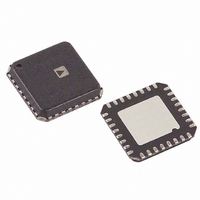
ADP1829ACPZ-R7 Analog Devices Inc, ADP1829ACPZ-R7 Datasheet - Page 21

ADP1829ACPZ-R7
Manufacturer Part Number
ADP1829ACPZ-R7
Description
IC BUCK SYNC ADJ 100uA 32LFCSP
Manufacturer
Analog Devices Inc
Type
Step-Down (Buck)r
Datasheet
1.ADP1829ACPZ-R7.pdf
(32 pages)
Specifications of ADP1829ACPZ-R7
Internal Switch(s)
No
Synchronous Rectifier
Yes
Number Of Outputs
2
Voltage - Output
0.6 ~ 15 V
Current - Output
100µA
Frequency - Switching
300kHz, 600kHz
Voltage - Input
3 ~ 18 V
Operating Temperature
-40°C ~ 125°C
Mounting Type
Surface Mount
Package / Case
32-LFCSP
Power - Output
1W
Primary Input Voltage
20V
No. Of Outputs
2
Output Voltage
17V
No. Of Pins
32
Operating Temperature Range
-40°C To +85°C
Msl
MSL 3 - 168 Hours
Frequency Max
1MHz
Termination Type
SMD
Lead Free Status / RoHS Status
Lead free / RoHS Compliant
For Use With
ADP1829-EVALZ - BOARD EVALUATION ADP1829
Lead Free Status / RoHS Status
Lead free / RoHS Compliant, Lead free / RoHS Compliant
Other names
ADP1829ACPZ-R7TR
Type II Compensator
If the output capacitor ESR zero frequency is sufficiently low (≤1/2
of the crossover frequency), use the ESR to stabilize the
regulator. In this case, use the circuit shown in Figure 28.
Calculate the compensation resistor, R
equation:
where:
f
V
Next choose the compensation capacitor to set the
compensation zero, f
frequency or 1/2 of the LC resonant frequency:
or
Solving for C
Solving for C
Use the larger value of C
Because of the finite output current drive of the error amplifier,
C
larger R
CO
RAMP
I
needs to be less than 10 nF. If it is larger than 10 nF, choose a
is chosen to be 1/10 of f
C
C
R =
f
f
is 1.3 V.
Z
Z
I
I
Z
1
1
FROM
V
TOP
=
=
OUT
=
=
π
π
and recalculate R
f
f
R
R
R
CO
4
2
LC
I
20
I
PHASE
Z
Z
TOP
1
R
in Equation 32 yields
in Equation 33 yields
–180°
–270°
f
f
R
=
TOP
=
SW
(dB)
LC
BOT
V
V
G
2
f
RAMP
40
Figure 28. Type II Compensation
π
SW
IN
R
1
Z1
Z
f
C
LC
, to the lesser of 1/4 of the crossover
=
f
I
R
ESR
2
2
I
Z
π
from Equation 34 or Equation 35.
f
Z
EA
SW.
R
C
1
f
HF
Z
Z
CO
VREF
C
and C
C
I
I
f
P
I
until C
COMP
Z
, with the following
0V
I
VRAMP
is less than 10 nF.
TO PWM
(31)
(32)
(33)
(34)
(35)
Rev. B | Page 21 of 32
Next choose the high frequency pole, f
Because C
Solving for C
Type III Compensator
If the output capacitor ESR zero frequency is greater than 1/2 of
the crossover frequency, use Type III compensator as shown in
Figure 29. Set the poles and zeros as follows:
or
Use the lower zero frequency from Equation 40 or Equation 41.
Calculate the compensator resistor, R
Next calculate C
C
C
FROM
R =
f
f
f
f
f
V
P1
P1
OUT
P1
Z1
Z
I
HF
Z
1
=
=
=
=
=
=
HF
=
π 2
R
1
2
2
f
f
f
<< C
PHASE
π
HF
π
P2
Z2
Z
TOP
R
R
–270°
f
f
R
2
R
1
–90°
R
(dB)
FF
SW
Z
SW
in Equation 36 and Equation 37 yields
TOP
BOT
1
Z
=
1
=
I
=
V
V
.
f
G
C
Z1
I
R
, Equation 29 is simplified to
RAMP
Figure 29. Type III Compensation
IN
1
2
HF
C
f
f
Z
CO
4
FF
2
LC
f
f
LC
SW
f
=
=
2
Z1
R
2
f
f
Z
f
40
CO
π
Z
SW
C
EA
R
HF
1
Z
VREF
=
C
C
I
I
2
f
P
π
R
Z
.
1
P1
Z
COMP
, to be 1/2 of f
C
I
0V
VRAMP
TO PWM
ADP1829
SW
.
(36)
(37)
(38)
(39)
(40)
(41)
(42)
(43)


