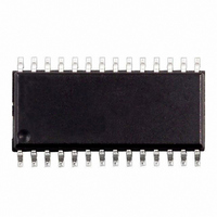
L6712ADTR STMicroelectronics, L6712ADTR Datasheet - Page 11

L6712ADTR
Manufacturer Part Number
L6712ADTR
Description
IC CTRLR DC/DC 2PH SYNC 28SOIC
Manufacturer
STMicroelectronics
Type
Step-Down (Buck)r
Datasheet
1.L6712AQTR.pdf
(29 pages)
Specifications of L6712ADTR
Internal Switch(s)
No
Synchronous Rectifier
Yes
Number Of Outputs
2
Voltage - Output
0.9 ~ 3.3 V
Current - Output
2A
Frequency - Switching
150kHz
Voltage - Input
12V
Operating Temperature
0°C ~ 70°C
Mounting Type
Surface Mount
Package / Case
28-SOIC (7.5mm Width)
Power - Output
2W
Operating Temperature Range
- 40 C to + 125 C
Mounting Style
SMD/SMT
Lead Free Status / RoHS Status
Contains lead / RoHS non-compliant
Other names
497-4218-2
L6712A L6712
3.3 DRIVER SECTION
The integrated high-current drivers allow using different types of power MOS (also multiple MOS to reduce
the R
), maintaining fast switching transition.
dsON
The drivers for the high-side mosfets use BOOTx pins for supply and PHASEx pins for return. The drivers
for the low-side mosfets use VCCDR pin for supply and PGND pin for return. A minimum voltage of 4.6V
at VCCDR pin is required to start operations of the device.
The controller embodies a sophisticated anti-shoot-through system to minimize low side body diode con-
duction time maintaining good efficiency saving the use of Schottky diodes in parallel to the LS mosfets.
The dead time is reduced to few nanoseconds assuring that high-side and low-side mosfets are never
switched on simultaneously: when the high-side mosfet turns off, the voltage on its source begins to fall;
when the voltage reaches 2V, the low-side mosfet gate drive is applied with 30ns delay. When the low-
side mosfet turns off, the voltage at LGATEx pin is sensed. When it drops below 1V, the high-side mosfet
gate drive is applied with a delay of 30ns. If the current flowing in the inductor is negative, the source of
high-side mosfet will never drop. To allow the turning on of the low-side mosfet even in this case, a watch-
dog controller is enabled: if the source of the high-side mosfet don't drop for more than 240ns, the low side
mosfet is switched on so allowing the negative current of the inductor to recirculate. This mechanism al-
lows the system to regulate even if the current is negative.
The BOOTx and VCCDR pins are separated from IC's power supply (VCC pin) as well as signal ground
(SGND pin) and power ground (PGND pin) in order to maximize the switching noise immunity. The sepa-
rated supply for the different drivers gives high flexibility in mosfet choice, allowing the use of logic-level
mosfet. Several combination of supply can be chosen to optimize performance and efficiency of the appli-
cation. Power conversion is also flexible; 5V or 12V bus can be chosen freely.
The peak current is shown for both the upper and the lower driver of the two phases in Figure 7. A 10nF
capacitive load has been used. For the upper drivers, the source current is 1.9A while the sink current is
1.5A with V
-V
= 12V; similarly, for the lower drivers, the source current is 2.4A while the sink
BOOT
PHASE
current is 2A with VCCDR = 12V.
Figure 7. Drivers peak current: High Side (left) and Low Side (right)
CH3 = HGATE1; CH4 = HGATE2
CH3 = LGATE1; CH4 = LGATE2
3.4 CURRENT READING AND OVER CURRENT
The current flowing trough each phase is read using the voltage drop across the low side mosfets R
dsON
or across a sense resistor (R
) in series to the LS mosfet and internally converted into a current. The
SENSE
transconductance ratio is issued by the external resistor Rg placed outside the chip between ISENx and
PGNDSx pins toward the reading points. The differential current reading rejects noise and allows to place
sensing element in different locations without affecting the measurement's accuracy. The current reading
11/29


