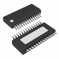
MAX1977EEI+ Maxim Integrated Products, MAX1977EEI+ Datasheet - Page 29

MAX1977EEI+
Manufacturer Part Number
MAX1977EEI+
Description
IC CNTRLR PS QUAD HI EFF 28QSOP
Manufacturer
Maxim Integrated Products
Datasheet
1.MAX1977EEIT.pdf
(32 pages)
Specifications of MAX1977EEI+
Applications
Controller, Notebook Computers
Voltage - Input
4.5 ~ 24 V
Number Of Outputs
4
Voltage - Output
3.3V, 5V, 2 ~ 5.5 V
Operating Temperature
0°C ~ 85°C
Mounting Type
Surface Mount
Package / Case
28-QSOP
Output Voltage
3.3 V, 2 V to 5.5 V
Input Voltage
6 V to 24 V
Mounting Style
SMD/SMT
Maximum Operating Temperature
+ 85 C
Minimum Operating Temperature
- 40 C
Case
SSOP
Dc
06+
Lead Free Status / RoHS Status
Lead free / RoHS Compliant
A coupled inductor or transformer can be substituted for
the inductor in the 5V or 3.3V SMPS to create an auxiliary
output (Figure 12). The MAX1777/MAX1977/MAX1999 are
particularly well suited for such applications because they
can be configured in ultrasonic or forced-PWM mode to
ensure good load regulation when the main supplies are
lightly loaded. An additional postregulation circuit can be
used to improve load regulation and limit output current.
The power requirements of the auxiliary supply must be
considered in the design of the main output. The trans-
former must be designed to deliver the required current
in both the primary and the secondary outputs with the
proper turns ratio and inductance. The power ratings of
the synchronous rectifier MOSFETs and the current limit
in the MAX1777/MAX1977/MAX1999 must also be
adjusted accordingly. Extremes of low input-output dif-
ferentials, widely different output loading levels, and high
turns ratios can further complicate the design due to par-
asitic transformer parameters such as interwinding
capacitance, secondary resistance, and leakage induc-
tance. Power from the main and secondary outputs is
combined to get an equivalent current referred to the
main output. Use this total current to determine the cur-
rent limit (see the Determining the Current Limit section):
where I
to the main output, and P
power from both the main output and the secondary
output:
where L
transformer turns ratio, V
rectified secondary voltage, V
across the secondary rectifier, V
value of the main output voltage, and V
state voltage drop across the synchronous rectifier
MOSFET. The transformer secondary return is often con-
nected to the main output voltage instead of ground in
order to reduce the necessary turns ratio. In this case,
subtract V
V
The secondary diode in coupled-inductor applications
must withstand flyback voltages greater than 60V, which
OUT
) in the transformer turns ratio equation above.
TOTAL
PRIMARY
L
Use of Coupled Inductors to Create
PRIMARY
Supply Controllers for Notebook Computers
OUT
I
TOTAL
High-Efficiency, Quad Output, Main Power-
is the equivalent output current referred
from the secondary voltage (V
N
is the primary inductance, N is the
______________________________________________________________________________________
=
=
=
V
V
OUT MIN
IN MAX
P
V
V
TOTAL
(
OUT IN MAX
SEC
TOTAL
SEC
(
(
)
+
V
)
× ƒ ×
is the minimum required
FWD
/
V
+
OUT(MIN)
is the sum of the output
(
FWD
V
Auxiliary Outputs
V
OUT
RECT
I
TOTAL
is the forward drop
)
−
V
RECT
is the minimum
OUT
×
LIR
is the on-
SEC
–
usually rules out most Schottky rectifiers. Common sili-
con rectifiers, such as the 1N4001, are also prohibited
because they are too slow. This often makes fast silicon
rectifiers such as the MURS120 the only choice. The fly-
back voltage across the rectifier is related to the V
V
where N is the transformer turns ratio (secondary wind-
ings/primary windings), V
DC output voltage, and V
put voltage. If the secondary winding is returned to V
instead of ground, subtract V
equation above. The diode’s reverse breakdown voltage
rating must also accommodate any ringing due to leak-
age inductance. The diode’s current rating should be at
least twice the DC load current on the secondary output.
The optional linear postregulator must be selected to
deliver the required load current from the transformer’s
rectified DC output. The linear regulator should be con-
figured to run close to dropout to minimize power dissi-
pation and should have good output accuracy under
those conditions. Input and output capacitors are cho-
sen to meet line regulation, stability, and transient
requirements. There are a wide variety of linear regula-
tors appropriate for this application; consult the specific
linear-regulator data sheet for details.
Widely different output loads effect load regulation. In
particular, when the secondary output is left unloaded
while the main output is fully loaded, the secondary out-
put capacitor may become overcharged by the leakage
inductance, reaching voltages much higher than intend-
ed. In this case, a minimum load or overvoltage protec-
tion may be required on the secondary output to protect
any device connected to this output.
Careful PC board layout is critical to achieve minimal
switching losses and clean, stable operation. This is
especially true when multiple converters are on the
same PC board where one circuit can affect the other.
The switching power stages require particular attention
(Figure 13). Refer to the MAX1999 EV kit data sheet for
a specific layout example.
Mount all of the power components on the top side of
the board with their ground terminals flush against one
another, if possible. Follow these guidelines for good
PC board layout:
• Isolate the power components on the top side from
OUT
the sensitive analog components on the bottom side
with a ground shield. Use a separate PGND plane
under the OUT3 and OUT5 sides (called PGND3 and
difference, according to the transformer turns ratio:
V
FLYBACK
PC Board Layout Guidelines
= V
SEC
SEC
OUT
+ (V
is the maximum secondary
OUT
is the primary (main) out-
IN
from V
- V
OUT
FLYBACK
)
✕
N
in the
OUT
IN
29
-


