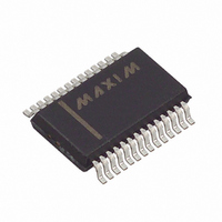
MAX1902EAI+ Maxim Integrated Products, MAX1902EAI+ Datasheet - Page 19

MAX1902EAI+
Manufacturer Part Number
MAX1902EAI+
Description
IC CNTRLR PWR SPLY LN 28-SSOP
Manufacturer
Maxim Integrated Products
Datasheet
1.MAX1904ETJ.pdf
(33 pages)
Specifications of MAX1902EAI+
Applications
Controller, Notebook Computers
Voltage - Input
4.2 ~ 30 V
Number Of Outputs
4
Voltage - Output
2.5 ~ 5 V
Operating Temperature
0°C ~ 85°C
Mounting Type
Surface Mount
Package / Case
28-SSOP
Output Voltage
3.3 V or 5 V or 2.5 V to 5.5 V
Output Current
5 A
Input Voltage
4.2 V to 30 V
Supply Current
5 uA
Switching Frequency
500 KHz
Mounting Style
SMD/SMT
Maximum Operating Temperature
+ 85 C
Minimum Operating Temperature
- 40 C
Lead Free Status / RoHS Status
Lead free / RoHS Compliant
Interference due to switching noise is reduced in PWM
mode by ensuring a constant switching frequency, thus
concentrating the emissions at a known frequency out-
side the system audio or IF bands. Choose an oscillator
frequency for which switching frequency harmonics
don’t overlap a sensitive frequency band. If necessary,
synchronize the oscillator to a tight-tolerance external
clock generator. To extend the output-voltage regula-
tion range, constant operating frequency is not main-
tained under overload or dropout conditions (see the
Dropout Operation section).
PWM mode (SKIP = high) forces two changes upon the
PWM controllers. First, it disables the minimum-current
comparator, ensuring fixed-frequency operation.
Second, it changes the detection threshold for reverse
current limit from 0 to -100mV, allowing the inductor cur-
rent to reverse at light loads. This results in fixed-fre-
quency operation and continuous inductor-current flow.
This eliminates discontinuous-mode inductor ringing and
improves cross regulation of transformer-coupled multi-
ple-output supplies, particularly in circuits that don’t use
additional secondary regulation via SECFB or V
In most applications, tie SKIP to GND to minimize qui-
escent supply current. VL supply current with SKIP high
is typically 30mA, depending on external MOSFET gate
capacitance and switching losses.
Soft-start allows a gradual increase of the internal cur-
rent-limit level at startup to reduce input surge currents.
Both SMPSs contain internal digital soft-start circuits,
each controlled by a counter, a digital-to-analog con-
verter (DAC), and a current-limit comparator. In shut-
down or standby mode, the soft-start counter is reset to
zero. When an SMPS is enabled, its counter starts
counting oscillator pulses, and the DAC begins incre-
menting the comparison voltage applied to the current-
limit comparator. The DAC output increases from 0 to
100mV in five equal steps as the count increases to
512 clocks. As a result, the main output capacitor
charges up relatively slowly. The exact time of the out-
put rise depends on output capacitance and load cur-
rent, and is typically 600µs with a 500kHz oscillator.
Dropout (low input-output differential operation) is
enhanced by stretching the clock pulse width to
increase the maximum duty factor. The algorithm fol-
lows: If the output voltage (V
tion without the current limit having been reached, the
SMPS skips an off-time period (extending the on-time).
At the end of the cycle, if the output is still out of regula-
tion, the SMPS skips another off-time period. This
500kHz Multi-Output, Low-Noise Power-Supply
Internal Digital Soft-Start Circuit
______________________________________________________________________________________
Controllers for Notebook Computers
OUT
Dropout Operation
) drops out of regula-
DD
.
action can continue until three off-time periods are
skipped, effectively dividing the clock frequency by as
much as four.
The typical PWM minimum off-time is 300ns, regardless
of the operating frequency. Lowering the operating fre-
quency raises the maximum duty factor above 97%.
Fixed, preset output voltages are selected when FB_ is
connected to ground. Adjusting the main output volt-
age with external resistors is simple for any of the
MAX1901/MAX1902/MAX1904, through resistor divi-
ders connected to FB3 and FB5 (Figure 2). Calculate
the output voltage with the following formula:
where V
The nominal output should be set approximately 1% or
2% high to make up for the MAX1901/MAX1902/
MAX1904 -2% typical load-regulation error. For exam-
ple, if designing for a 3.0V output, use a resistor ratio
that results in a nominal output voltage of 3.05V. This
slight offsetting gives the best possible accuracy.
Recommended normal values for R2 range from 5kΩ to
100kΩ. To achieve a 2.5V nominal output, simply con-
nect FB_ directly to CSL_.
Remote output-voltage sensing, while not possible in
fixed-output mode due to the combined nature of the
voltage-sense and current-sense inputs (CSL3 and
CSL5), is easy to do in adjustable mode by using the top
of the external resistor-divider as the remote sense point.
When using adjustable mode, it is a good idea to
always set the “3.3V output” to a lower voltage than the
“5V output.” The 3.3V output must always be less than
VL, so that the voltage on CSH3 and CSL3 is within the
common-mode range of the current-sense inputs. While
VL is nominally 5V, it can be as low as 4.7V when lin-
early regulating, and as low as 4.2V when automatically
bootstrapped to CSH5.
A flyback-winding control loop regulates a secondary
winding output, improving cross-regulation when the
primary output is lightly loaded or when there is a low
input-output differential voltage. If V
below its regulation threshold, the low-side switch is
turned on for an extra 0.75µs. This reverses the induc-
Secondary Feedback Regulation Loop
REF
= 2.5V nominal.
V
OUT
Adjustable-Output Feedback
= V
REF
(1 + R1 / R2)
(SECFB or V
(Dual Mode FB)
DD
or SECFB falls
DD
19
)


