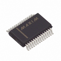
MAX1902EAI+ Maxim Integrated Products, MAX1902EAI+ Datasheet - Page 13

MAX1902EAI+
Manufacturer Part Number
MAX1902EAI+
Description
IC CNTRLR PWR SPLY LN 28-SSOP
Manufacturer
Maxim Integrated Products
Datasheet
1.MAX1904ETJ.pdf
(33 pages)
Specifications of MAX1902EAI+
Applications
Controller, Notebook Computers
Voltage - Input
4.2 ~ 30 V
Number Of Outputs
4
Voltage - Output
2.5 ~ 5 V
Operating Temperature
0°C ~ 85°C
Mounting Type
Surface Mount
Package / Case
28-SSOP
Output Voltage
3.3 V or 5 V or 2.5 V to 5.5 V
Output Current
5 A
Input Voltage
4.2 V to 30 V
Supply Current
5 uA
Switching Frequency
500 KHz
Mounting Style
SMD/SMT
Maximum Operating Temperature
+ 85 C
Minimum Operating Temperature
- 40 C
Lead Free Status / RoHS Status
Lead free / RoHS Compliant
Table 2. Component Suppliers
The MAX1901/MAX1902/MAX1904 contain ten major
circuit blocks (Figure 2).
The two pulse-width-modulation (PWM) controllers
each consist of a Dual Mode feedback network and
multiplexer, a multi-input PWM comparator, high-side
and low-side gate drivers, and logic. MAX1901/
MAX1902 contain fault-protection circuits that monitor
the main PWM outputs for undervoltage and overvolt-
age. A power-on sequence block controls the power-
up timing of the main PWMs and determines whether
one or both of the outputs are monitored for undervoltage
faults. The MAX1902 includes a secondary feedback net-
work and 12V linear regulator to generate a 12V output
from a coupled-inductor flyback winding. The
MAX1901/MAX1904 have a secondary feedback input
(SECFB) instead, which allows a quasi-regulated,
adjustable output, coupled-inductor flyback winding to be
attached to either the 3.3V or the 5V main inductor. Bias
generator blocks include the 5V IC internal rail (V
regulator, 2.5V precision reference, and automatic boot-
strap switchover circuit. The PWMs share a common
333kHz/500kHz synchronizable oscillator.
These internal IC blocks aren’t powered directly from
the battery. Instead, the 5V V
down the battery voltage to supply both V
gate drivers. The synchronous-switch gate drivers are
directly powered from V
gate drivers are indirectly powered from V
external diode-capacitor boost circuit. An automatic
bootstrap circuit turns off the 5V linear regulator and
powers the IC from the 5V PWM output voltage if the
output is above 4.5V.
The two PWM controllers are nearly identical. The only
differences are fixed output settings (3.3V vs. 5V), the
VL/CSL5 bootstrap switch connected to the 5V PWM,
and SECFB. The heart of each current-mode PWM con-
troller is a multi-input, open-loop comparator that sums
Dale-Vishay
Fairchild
Semiconductor
International
Rectifier
Sanyo
Sumida
Taiyo Yuden
MANUFACTURER
500kHz Multi-Output, Low-Noise Power-Supply
______________________________________________________________________________________
402-564-3131
408-721-2181
310-322-3331
619-661-6835
847-956-0666
408-573-4150
USA PHONE
L
, while the high-side switch
PWM Controller Block
Controllers for Notebook Computers
L
linear regulator steps
FACTORY FAX
402-563-6418
408-721-1635
310-322-3332
619-661-1055
847-956-0702
408-573-4159
L
L
and the
L
) linear
via an
three signals: the output-voltage error signal with
respect to the reference voltage, the current-sense sig-
nal, and the slope-compensation ramp (Figure 3). The
PWM controller is a direct-summing type, lacking a tra-
ditional error amplifier and the phase shift associated
with it. This direct-summing configuration approaches
ideal cycle-by-cycle control over the output voltage.
When SKIP = low, Idle Mode circuitry automatically
optimizes efficiency throughout the load current range.
Idle Mode dramatically improves light-load efficiency
by reducing the effective frequency, which reduces
switching losses. It keeps the peak inductor current
above 25% of the full current limit in an active cycle,
allowing subsequent cycles to be skipped. Idle Mode
transitions seamlessly to fixed-frequency PWM opera-
tion as load current increases.
With SKIP = high, the controller always operates in fixed-
frequency PWM mode for lowest noise. Each pulse from
the oscillator sets the main PWM latch that turns on the
high-side switch for a period determined by the duty fac-
tor (approximately V
turns off, the synchronous rectifier latch sets; 60ns later,
the low-side switch turns on. The low-side switch stays on
until the beginning of the next clock cycle.
In PWM mode, the controller operates as a fixed-fre-
quency current-mode controller where the duty ratio is
set by the input/output voltage ratio. The current-mode
feedback system regulates the peak inductor current
value as a function of the output-voltage error signal. In
continuous-conduction mode, the average inductor
current is nearly the same as the peak current, so the
circuit acts as a switch-mode transconductance ampli-
fier. This pushes the second output LC filter pole, nor-
mally found in a duty-factor-controlled (voltage-mode)
PWM, to a higher frequency. To preserve inner-loop
stability and eliminate regenerative inductor current
“staircasing”, a slope-compensation ramp is summed
into the main PWM comparator to make the apparent
duty factor less than 50%.
The MAX1901/MAX1902/MAX1904 use a relatively low
loop gain, allowing the use of lower-cost output capaci-
tors. The relative gains of the voltage-sense and cur-
rent-sense inputs are weighted by the values of current
sources that bias three differential input stages in the
main PWM comparator (Figure 4). The relative gain of
the voltage comparator to the current comparator is
internally fixed at K = 2:1. The low loop gain results in
the 2% typical load-regulation error. The low value of
loop gain helps reduce output filter capacitor size and
cost by shifting the unity-gain crossover frequency to a
lower level.
OUT
/ V
IN
). As the high-side switch
13


