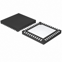
MAX8760ETL+T Maxim Integrated Products, MAX8760ETL+T Datasheet - Page 37

MAX8760ETL+T
Manufacturer Part Number
MAX8760ETL+T
Description
IC CNTRLR QUICK PWM 40-TQFN
Manufacturer
Maxim Integrated Products
Datasheet
1.MAX8760ETL.pdf
(39 pages)
Specifications of MAX8760ETL+T
Applications
Controller, 6-bit VID AMD Mobile Turion™
Voltage - Input
4 ~ 28 V
Number Of Outputs
2
Voltage - Output
0.38 ~ 1.55 V
Operating Temperature
0°C ~ 85°C
Mounting Type
Surface Mount
Package / Case
40-TQFN Exposed Pad
Output Voltage
0.375 V to 1.55 V
Output Current
4000 mA
Mounting Style
SMD/SMT
Switching Frequency
550 KHz
Maximum Operating Temperature
+ 100 C
Minimum Operating Temperature
- 40 C
Synchronous Pin
No
Topology
Buck
Lead Free Status / RoHS Status
Lead free / RoHS Compliant
Careful PC board layout is critical to achieve low
switching losses and clean, stable operation. The
switching power stage requires particular attention
(Figure 11). If possible, mount all the power compo-
nents on the top side of the board with their ground ter-
minals flush against one another. Follow these
guidelines for good PC board layout:
1)
2)
3)
4)
5)
6)
7)
Keep the high-current paths short, especially at
the ground terminals. This is essential for stable,
jitter-free operation.
Connect all analog grounds to a separate solid
copper plane, which connects to the GND pin of
the Quick-PWM controller. This includes the V
bypass capacitor, REF and GNDS bypass capaci-
tors, compensation (CC_) components, and the
resistive dividers connected to ILIM and OFS.
Each slave controller should also have a separate
analog ground. Return the appropriate noise-sen-
sitive slave components to this plane. Since the
reference in the master is sometimes connected
to the slave, it may be necessary to couple the
analog ground in the master to the analog ground
in the slave to prevent ground offsets. A low-value
(≤10Ω) resistor is sufficient to link the two grounds.
Keep the power traces and load connections short.
This is essential for high efficiency. The use of thick
copper PC boards (2oz vs. 1oz) can enhance
full-load efficiency by 1% or more. Correctly routing
PC board traces is a difficult task that must be ap-
proached in terms of fractions of centimeters, where
a single mΩ of excess trace resistance causes a
measurable efficiency penalty.
Keep the high-current, gate-driver traces (DL, DH,
LX, and BST) short and wide to minimize trace
resistance and inductance. This is essential for
high-power MOSFETs that require low-impedance
gate drivers to avoid shoot-through currents.
C_P, C_N, OAIN+, and OAIN- connections for cur-
rent limiting and voltage positioning must be made
using Kelvin-sense connections to guarantee the
current-sense accuracy.
When trade-offs in trace lengths must be made, it
is preferable to allow the inductor-charging path to
be made longer than the discharge path. For
example, it is better to allow some extra distance
between the input capacitors and the high-side
MOSFET than to allow distance between the
Dual-Phase, Quick-PWM Controller for AMD
Applications Information
Mobile Turion 64 CPU Core Power Supplies
______________________________________________________________________________________
PC Board Layout Guidelines
CC
8)
Place the power components first, with ground termi-
nals adjacent (low-side MOSFET source, C
and D1 anode). If possible, make all these connections
on the top layer with wide, copper-filled areas.
1)
2)
3)
4)
TRANSISTOR COUNT: 11,015
PROCESS: BiCMOS
inductor and the low-side MOSFET or between the
inductor and the output filter capacitor.
Route high-speed switching nodes away from
sensitive analog areas (REF, CCV, CCI, FB, C_P,
C_N, etc). Make all pin-strap control input connec-
tions (SHDN, ILIM, SKIP, SUS, S_, TON) to analog
ground or V
Mount the controller IC adjacent to the low-side
MOSFET. The DL gate traces must be short and
wide (50 mils to 100 mils wide if the MOSFET is
1in from the controller IC).
Group the gate-drive components (BST diodes
and capacitors, V
near the controller IC.
Make the DC-to-DC controller ground connections
as shown in the Standard Application Circuits.
This diagram can be viewed as having four sepa-
rate ground planes: input/output ground, where all
the high-power components go; the power ground
plane, where the PGND pin and V
capacitor go; the master’s analog ground plane,
where sensitive analog components, the master’s
GND pin, and V
slave’s analog ground plane, where the slave’s
GND pin and V
ter’s GND plane must meet the PGND plane only
at a single point directly beneath the IC. Similarly,
the slave’s GND plane must meet the PGND plane
only at a single point directly beneath the IC. The
respective master and slave ground planes
should connect to the high-power output ground
with a short metal trace from PGND to the source
of the low-side MOSFET (the middle of the star
ground). This point must also be very close to the
output capacitor ground terminal.
Connect the output power planes (V
system ground planes) directly to the output filter
capacitor positive and negative terminals with
multiple vias. Place the entire DC-to-DC converter
circuit as close to the CPU as is practical.
CC
rather than power ground or V
CC
CC
DD
bypass capacitor go. The mas-
bypass capacitor go; and the
bypass capacitor) together
Chip Information
Layout Procedure
DD
CORE
IN
, C
bypass
DD
OUT
and
37
.
,


