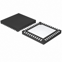
MAX8760ETL+T Maxim Integrated Products, MAX8760ETL+T Datasheet - Page 28

MAX8760ETL+T
Manufacturer Part Number
MAX8760ETL+T
Description
IC CNTRLR QUICK PWM 40-TQFN
Manufacturer
Maxim Integrated Products
Datasheet
1.MAX8760ETL.pdf
(39 pages)
Specifications of MAX8760ETL+T
Applications
Controller, 6-bit VID AMD Mobile Turion™
Voltage - Input
4 ~ 28 V
Number Of Outputs
2
Voltage - Output
0.38 ~ 1.55 V
Operating Temperature
0°C ~ 85°C
Mounting Type
Surface Mount
Package / Case
40-TQFN Exposed Pad
Output Voltage
0.375 V to 1.55 V
Output Current
4000 mA
Mounting Style
SMD/SMT
Switching Frequency
550 KHz
Maximum Operating Temperature
+ 100 C
Minimum Operating Temperature
- 40 C
Synchronous Pin
No
Topology
Buck
Lead Free Status / RoHS Status
Lead free / RoHS Compliant
Dual-Phase, Quick-PWM Controller for AMD
Mobile Turion 64 CPU Core Power Supplies
Together, the feedback-sense resistor (R
GNDS input sum the remote-sense voltages with the
feedback signals that set the voltage-positioned output,
enabling true differential remote sense of the processor
voltage. Connect the feedback-sense resistor (R
and ground-sense input (GNDS) directly to the proces-
sor’s core supply remote-sense outputs as shown in the
Standard Applications Circuit.
The multiphase Quick-PWM controllers include a third
amplifier used to add small offsets to the voltage-posi-
tioned load line. The offset amplifier is summed directly
with the feedback voltage, making the offset gain inde-
pendent of the DAC code. This amplifier has the ability
to offset the output by ±100mV.
The offset is adjusted using resistive voltage-dividers at
the OFS input. For inputs from 0 to 0.8V, the offset
amplifier adds a negative offset to the output that is
equal to 1/8 the voltage appearing at the selected OFS
input (V
1.2V to 2V, the offset amplifier adds a positive offset to
the output that is equal to 1/8th the difference between
the reference voltage and the voltage appearing at the
selected OFS input (V
V
positive and negative offsets with a single input. The
piecewise linear transfer function is shown in the
Typical Operating Characteristics. The regions of the
transfer function below zero, above 2V, and between
0.8V and 1.2V are undefined. OFS inputs are disal-
lowed in these regions, and the respective effects on
the output are not specified.
The controller disables the offset amplifier during sus-
pend mode (SUS = REF or high).
Table 7.
*Settings for a dual 180° out-of-phase controller.
28
OFS
CONNECTION
(3.3V or V
______________________________________________________________________________________
)). With this scheme, the controller supports both
SKIP
GND
High
REF
OUT
CC
S S K K I I P P Settings*
= V
)
DAC
pulse skipping
pulse skipping
forced PWM
One-phase
Two-phase
Two-phase
- 0.125 x V
MODE
OUT
= V
DAC
OFS
The controller operates with a constant switching frequency, providing low-noise forced-PWM
operation. The controller disables the zero-crossing comparators, forcing the low-side gate-
drive waveform to be constantly the complement of the high-side gate-drive waveform.
The controller automatically switches over to PFM operation under light loads. The controller
keeps both phases active and uses the automatic pulse-skipping control scheme, alternating
between the primary and secondary phases with each cycle.
The controller automatically switches over to PFM operation under light loads. Only the main
phase is active. The secondary phase is disabled, DLS and DHS are pulled low, so LXS is
high impedance.
+ 0.125 x (V
). For inputs from
Offset Amplifier
FBS
) and
REF
FBS
)
-
During normal mode, when the CPU is actively running
(SKIP = high, Table 7), the Quick-PWM controller oper-
ates with the low-noise forced-PWM control scheme.
Forced-PWM operation disables the zero-crossing
comparator, forcing the low-side gate-drive waveform
to be constantly the complement of the high-side gate-
drive waveform. This keeps the switching frequency
fairly constant and allows the inductor current to
reverse under light loads, providing fast, accurate neg-
ative output voltage transitions by quickly discharging
the output capacitors.
Forced-PWM operation comes at a cost: the no-load 5V
bias supply current remains between 10mA to 60mA
per phase, depending on the external MOSFETs and
switching frequency. To maintain high efficiency under
light-load conditions, the processor may switch the
controller to a low-power pulse-skipping control
scheme after entering suspend mode.
Figure 6. Offset Voltage
Forced-PWM Operation (Normal Mode)
OPERATION
-100
-200
200
100
0
0
0.5
OFS VOLTAGE (V)
0.8
1.0
1.2
UNDEFINED
REGION
1.5
2.0


