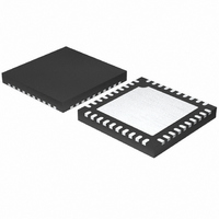
MAX8760ETL+T Maxim Integrated Products, MAX8760ETL+T Datasheet - Page 27

MAX8760ETL+T
Manufacturer Part Number
MAX8760ETL+T
Description
IC CNTRLR QUICK PWM 40-TQFN
Manufacturer
Maxim Integrated Products
Datasheet
1.MAX8760ETL.pdf
(39 pages)
Specifications of MAX8760ETL+T
Applications
Controller, 6-bit VID AMD Mobile Turion™
Voltage - Input
4 ~ 28 V
Number Of Outputs
2
Voltage - Output
0.38 ~ 1.55 V
Operating Temperature
0°C ~ 85°C
Mounting Type
Surface Mount
Package / Case
40-TQFN Exposed Pad
Output Voltage
0.375 V to 1.55 V
Output Current
4000 mA
Mounting Style
SMD/SMT
Switching Frequency
550 KHz
Maximum Operating Temperature
+ 100 C
Minimum Operating Temperature
- 40 C
Synchronous Pin
No
Topology
Buck
Lead Free Status / RoHS Status
Lead free / RoHS Compliant
Without active current-balance circuitry, the current
matching between phases depends on the MOSFET’s
on-resistance (R
matching, and inductance matching. For example, vari-
ation in the low-side MOSFET on-resistance (ignoring
thermal effects) results in a current mismatch that is
proportional to the on-resistance difference:
However, mismatches between on-times, off-times, and
inductor values increase the worst-case current imbal-
ance, making it impossible to passively guarantee
accurate current balancing.
The multiphase Quick-PWM controller integrates the dif-
ference between the current-sense voltages and
adjusts the on-time of the secondary phase to maintain
current balance. The current balance now relies on the
accuracy of the current-sense resistors instead of the
inaccurate, thermally sensitive on-resistance of the low-
side MOSFETs.
With active current balancing, the current mismatch is
determined by the current-sense resistor values and the
offset voltage of the transconductance amplifiers:
where V
tion in the Electrical Characteristics table.
The worst-case current mismatch occurs immediately
after a load transient due to inductor value mismatches,
resulting in different di/dt for the two phases. The time it
takes the current-balance loop to correct the transient
imbalance depends on the mismatch between the
inductor values and switching frequency.
The multiphase Quick-PWM controllers include an inde-
pendent operational amplifier for adding gain to the volt-
age-positioning sense path. The voltage-positioning gain
allows the use of low-value current-sense resistors to
minimize power dissipation. This 3MHz gain-bandwidth
amplifier was designed with low offset voltage (70µV typ)
to meet the IMVP output-accuracy requirements.
OS(IBAL)
I
I
MAIN
OS IBAL
Feedback Adjustment Amplifiers
(
Dual-Phase, Quick-PWM Controller for AMD
Mobile Turion 64 CPU Core Power Supplies
DS(ON)
-
is the current balance offset specifica-
I
2
______________________________________________________________________________________
)
ND
=
=
I
LM
), thermal ballasting, on-/off-time
Voltage-Positioning Amplifier
I
MAIN
-
I
LS
⎡
⎢
⎢
⎣
1
=
-
⎛
⎜
⎝
V
Current Balance
R
R
OS IBAL
R
SENSE
MAIN
2
(
ND
⎞
⎟
⎠
)
⎤
⎥
⎥
⎦
The inverting (OAIN-) and noninverting (OAIN+) inputs
are used to differentially sense the voltage across the
voltage-positioning sense resistor. The op amp’s output is
internally connected to the regulator’s feedback input
(FB). The op amp should be configured as a noninvert-
ing, differential amplifier, as shown in Figure 10. The
voltage-positioning slope is set by properly selecting the
feedback resistor connected from FB to OAIN- (see the
Setting Voltage Positioning section). For applications
using a slave controller, additional differential input
resistors (summing configuration) can be connected to
the slave’s voltage-positioning sense resistor. Summing
together both the master and slave current-sense signals
ensures that the voltage-positioning slope remains con-
stant when the slave controller is disabled.
The controller also uses the amplifier for remote output
sensing (FBS) by summing in the remote-sense voltage
into the positive terminal of the voltage-positioning
amplifier (Figure 10).
In applications that do not require voltage-positioning
gain, the amplifier can be disabled by connecting the
OAIN- pin directly to V
put becomes high impedance, guaranteeing that the
unused amplifier does not corrupt the FB input signal.
The logic threshold to disable the op amp is approxi-
mately V
A feedback amplifier forces the DC average of the
feedback voltage to equal the VID DAC setting. This
transconductance amplifier integrates the feedback
voltage and provides a fine adjustment to the regulation
voltage (Figure 5), allowing accurate DC output voltage
regulation regardless of the output ripple voltage. The
feedback amplifier has the ability to shift the output
voltage. The differential input voltage range is at least
±80mV total, including DC offset and AC ripple. The
integration time constant can be set easily with an
external compensation capacitor at the CCV pin. Use a
capacitor value of 47pF to 1000pF (150pF typ).
The multiphase Quick-PWM controllers include differen-
tial remote-sense inputs to eliminate the effects of volt-
age drops down the PC board traces and through the
processor’s power pins. The remote output sense (FBS)
is accomplished by summing in the remote-sense volt-
age into the positive terminal of the voltage-positioning
amplifier (Figure 10). The controller includes a dedicat-
ed input and internal amplifier for the remote ground
sense. The GNDS amplifier adds an offset directly to
the feedback voltage, adjusting the output voltage to
counteract the voltage drop in the ground path.
CC
- 1V.
CC
. The disabled amplifier’s out-
Differential Remote Sense
Integrator Amplifier
27


