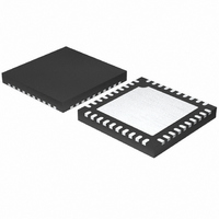
MAX8760ETL+T Maxim Integrated Products, MAX8760ETL+T Datasheet - Page 34

MAX8760ETL+T
Manufacturer Part Number
MAX8760ETL+T
Description
IC CNTRLR QUICK PWM 40-TQFN
Manufacturer
Maxim Integrated Products
Datasheet
1.MAX8760ETL.pdf
(39 pages)
Specifications of MAX8760ETL+T
Applications
Controller, 6-bit VID AMD Mobile Turion™
Voltage - Input
4 ~ 28 V
Number Of Outputs
2
Voltage - Output
0.38 ~ 1.55 V
Operating Temperature
0°C ~ 85°C
Mounting Type
Surface Mount
Package / Case
40-TQFN Exposed Pad
Output Voltage
0.375 V to 1.55 V
Output Current
4000 mA
Mounting Style
SMD/SMT
Switching Frequency
550 KHz
Maximum Operating Temperature
+ 100 C
Minimum Operating Temperature
- 40 C
Synchronous Pin
No
Topology
Buck
Lead Free Status / RoHS Status
Lead free / RoHS Compliant
cuit longevity.
Most of the following MOSFET guidelines focus on the
challenge of obtaining high load-current capability
when using high-voltage (>20V) AC adapters. Low-cur-
rent applications usually require less attention.
The high-side MOSFET (N
the resistive losses plus the switching losses at both
V
Ideally, the losses at V
losses at V
losses at V
at V
R
at V
V
R
range, the minimum power dissipation occurs where the
resistive losses equal the switching losses.
Choose a low-side MOSFET that has the lowest possible
on-resistance (R
package (i.e., one or two 8-pin SOs, DPAK, or D
and is reasonably priced. Ensure that the DL gate driver
can supply sufficient current to support the gate charge
and the current injected into the parasitic gate-to-drain
capacitor caused by the high-side MOSFET turning on;
otherwise, cross-conduction problems can occur (see
the MOSFET Gate Driver section).
Worst-case conduction losses occur at the duty factor
extremes. For the high-side MOSFET (N
case power dissipation due to resistance occurs at the
minimum input voltage:
where η
Generally, a small high-side MOSFET is desired to
reduce switching losses at high input voltages.
However, the R
power dissipation often limits how small the MOSFET
can be. Again, the optimum occurs when the switching
losses equal the conduction (R
side switching losses do not usually become an issue
until the input is greater than approximately 15V.
Calculating the power dissipation in high-side MOSFET
(N
allow for difficult quantifying factors that influence the
turn-on and turn-off times. These factors include the
internal gate resistance, gate charge, threshold
Dual-Phase, Quick-PWM Controller for AMD
Mobile Turion 64 CPU Core Power Supplies
34
PD N RESISTIVE
IN(MIN)
DS(ON)
IN(MIN)
DS(ON)
H
IN(MAX)
) due to switching losses is difficult since it must
IN(MAX)
(
______________________________________________________________________________________
H
TOTAL
, consider reducing the size of N
but with higher C
to lower C
and V
IN(MIN)
, consider increasing the size of N
IN(MAX)
are significantly higher than the losses at
is the total number of phases.
IN(MAX)
DS(ON)
DS(ON)
are significantly higher than the losses
, with lower losses in between. If the
GATE
)
MOSFET Power Dissipation
=
IN(MIN)
Power MOSFET Selection
. Calculate both of these sums.
). If V
required to stay within package
⎛
⎜
⎝
), comes in a moderate-sized
V
GATE
V
OUT
H
IN
) must be able to dissipate
IN
should be roughly equal to
). Conversely, if the losses
does not vary over a wide
⎞
⎟
⎠
⎛
⎜
⎝
DS(ON)
η
I
LOAD
TOTAL
) losses. High-
H
H
⎞
⎟
⎠
), the worst-
2
H
(increasing
R
(reducing
DS ON
2
(
PAK),
)
voltage, source inductance, and PC board layout
characteristics. The following switching-loss calculation
provides only a very rough estimate and is no substi-
tute for breadboard evaluation, preferably including
verification using a thermocouple mounted on N
where C
and I
(1A typ).
Switching losses in the high-side MOSFET can become
an insidious heat problem when maximum AC adapter
voltages are applied due to the squared term in the C x
V
MOSFET chosen for adequate R
voltages becomes extraordinarily hot when biased from
V
lower parasitic capacitance.
For the low-side MOSFET (N
dissipation always occurs at maximum input voltage:
The worst-case for MOSFET power dissipation occurs
under heavy overloads that are greater than
I
the current limit and cause the fault latch to trip. To pro-
tect against this possibility, you can “overdesign” the
circuit to tolerate:
where I
allowed by the current-limit circuit, including threshold
tolerance and on-resistance variation. The MOSFETs
must have a good-size heatsink to handle the overload
power dissipation.
Choose a Schottky diode (D
low enough to prevent the low-side MOSFET body
diode from turning on during the dead time. As a gen-
eral rule, select a diode with a DC current rating equal
to 1/3 of the load current-per-phase. This diode is
optional and can be removed if efficiency is not critical.
The boost capacitors (C
enough to handle the gate-charging requirements of
the high-side MOSFETs. Typically, 0.1µF ceramic
PD N SWITCHING
PD N RESISTIVE
LOAD(MAX)
IN
IN(MAX)
2
(
(
GATE
x f
I
L
H
LOAD
VALLEY(MAX)
SW
RSS
, consider choosing another MOSFET with
=
=
is the peak gate-drive source/sink current
switching-loss equation. If the high-side
but are not quite high enough to exceed
is the reverse transfer capacitance of N
η
η
TOTAL
TOTAL VALLEY MAX
)
=
)
⎡
⎢
⎣
I
=
⎛
⎜
⎝
1
I
VALLEY MAX
(
−
is the maximum valley current
V
IN MAX
⎛
⎜
⎝
V
BST
(
IN MAX
V
(
OUT
(
(
) must be selected large
L
L
)
)
) with a forward voltage
), the worst-case power
)
2
)
)
+
⎛
⎜
⎝
Boost Capacitors
⎞
⎟
⎠
+
DS(ON)
C
⎤
⎥
⎦
⎛
⎜
⎝
I
I
RSS SW
⎛
⎜
⎝
∆
LOAD MAX
GATE
I
η
INDUCTOR
I
TOTAL
LOAD
f
2
(
2
at low battery
⎞
⎟
⎠
⎛
⎜
⎝
⎞
⎟
⎠
)
LIR
2
η
I
⎞
⎟
⎠
TOTAL
R
LOAD
H
DS ON
⎞
⎟
⎠
:
(
⎞
⎟
⎠
)
H


