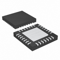
MAX8550ETI+ Maxim Integrated Products, MAX8550ETI+ Datasheet - Page 3

MAX8550ETI+
Manufacturer Part Number
MAX8550ETI+
Description
IC PWR SUP DDR INTEG 28TQFN
Manufacturer
Maxim Integrated Products
Datasheet
1.MAX8550ETIT.pdf
(29 pages)
Specifications of MAX8550ETI+
Applications
Controller, DDR
Voltage - Input
2 ~ 28 V
Number Of Outputs
2
Voltage - Output
1.8V, 2.5V, 0.7 ~ 5.5 V
Operating Temperature
-40°C ~ 85°C
Mounting Type
Surface Mount
Package / Case
28-TQFN Exposed Pad
Output Voltage
0.7 V to 5.5 V, 1.8 V, 2.5 V
Output Current
20 A
Input Voltage
2 V to 28 V
Mounting Style
SMD/SMT
Maximum Operating Temperature
+ 85 C
Minimum Operating Temperature
- 40 C
Lead Free Status / RoHS Status
Lead free / RoHS Compliant
ELECTRICAL CHARACTERISTICS (continued)
(V
= GND, PGND1 = PGND2 = LX = GND, TON = OPEN, V
are at T
REFERENCE
Reference Voltage
Reference Load Regulation
REF Undervoltage Lockout
FAULT DETECTION
OVP Trip Threshold
(Referred to Nominal V
UVP Trip Threshold
(Referred to Nominal V
POK1 Trip Threshold
(Referred to Nominal V
POK2 Trip Threshold
(Referred to Nominal V
and V
UVP Blanking Time
OVP, UVP, POK_ Propagation
Delay
POK_ Output Low Voltage
POK_ Leakage Current
ILIM Adjustment Range
ILIM Input Leakage Current
Current-Limit Threshold (Fixed)
PGND1 to LX
Current-Limit Threshold
(Adjustable) PGND1 to LX
Current-Limit Threshold (Negative
Direction) PGND1 to LX
Current-Limit Threshold (Negative
Direction) PGND1 to LX
Zero-Crossing Detection
Threshold PGND1 to LX
Thermal-Shutdown Threshold
Thermal-Shutdown Hysteresis
IN
= +15V, V
VTTR
A
= +25°C.) (Note 1)
PARAMETER
)
Integrated DDR Power-Supply Solutions for
DD
= AV
Desktops, Notebooks, and Graphic Cards
_______________________________________________________________________________________
DD
OUT
OUT
OUT
VTTS
= V
)
)
)
SHDNA
SYMBOL
= V
V
V
SHDNB
ILIM
REF
= V
I
AV
V
Hysteresis
UVP/OVP = AVDD (Note 4)
Lower level, falling edge, 1% hysteresis
Upper level, rising edge, 1% hysteresis
Lower level, falling edge, 1% hysteresis
Upper level, rising edge, 1% hysteresis
From rising edge of SHDNA
OVP not applicable in MAX8551
I
V
V
SKIP = AV
SKIP = AV
REF
SINK
REF
POK_
ILIM
BST
DD
= 0 to 50µA
rising
= 4mA
= 2V
= 4.5V to 5.5V; I
= V
= 5.5V, V
VTTS
ILIM
DD
DD
, V
= V
(Note 4)
= 5V, V
CONDITIONS
ILIM
FB
VTT
= 0.8V, V
, T
= 2V (Note 4)
OUT
REF
A
= -40°C to +85°C, unless otherwise noted. Typical values
= 0
= V
VTTS
REFIN
= 1.3V
= V
VTTI
= 2.5V, UVP/OVP = STBY = FB = SKIP
107.5
MIN
1.98
87.5
0.25
112
107
170
-75
65
87
10
45
+160
TYP
-250
1.93
300
116
110
110
200
-60
70
90
90
20
10
50
15
2
3
112.5
MAX
2.02
0.01
92.5
2.00
120
113
235
0.3
0.1
-45
75
93
40
55
1
UNITS
mV
mV
mV
mV
mV
mV
ms
µA
µA
°C
°C
µs
%
%
%
%
V
V
V
V
V
3


