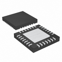
MAX8550ETI+ Maxim Integrated Products, MAX8550ETI+ Datasheet - Page 17

MAX8550ETI+
Manufacturer Part Number
MAX8550ETI+
Description
IC PWR SUP DDR INTEG 28TQFN
Manufacturer
Maxim Integrated Products
Datasheet
1.MAX8550ETIT.pdf
(29 pages)
Specifications of MAX8550ETI+
Applications
Controller, DDR
Voltage - Input
2 ~ 28 V
Number Of Outputs
2
Voltage - Output
1.8V, 2.5V, 0.7 ~ 5.5 V
Operating Temperature
-40°C ~ 85°C
Mounting Type
Surface Mount
Package / Case
28-TQFN Exposed Pad
Output Voltage
0.7 V to 5.5 V, 1.8 V, 2.5 V
Output Current
20 A
Input Voltage
2 V to 28 V
Mounting Style
SMD/SMT
Maximum Operating Temperature
+ 85 C
Minimum Operating Temperature
- 40 C
Lead Free Status / RoHS Status
Lead free / RoHS Compliant
The VTT output is a linear regulator that regulates the
input (VTTI) to half the V
point for VTT is at the VTTS input (Figure 1). VTT is
capable of sinking and sourcing at least 1.5A of continu-
ous current and 3A peak current. The current limit for
VTT and VTTR is typically ±5A and ±40mA, respective-
ly. When the current limit for either output is reached,
the outputs regulate the current, not the voltage.
The MAX8550/MAX8551 provide overvoltage/undervolt-
age fault protection in the buck controller. Select
OVP/UVP to enable and disable fault protection as
shown in Table 3. Once activated, the controller contin-
uously monitors the output for undervoltage and over-
voltage fault conditions.
When the output voltage rises above 116% of the nomi-
nal regulation voltage (MAX8550 only) and OVP is
enabled (OVP/UVP = AV
sets the fault latch, shuts down the PWM controller, and
immediately pulls DH low and forces DL high. This
turns on the synchronous-rectifier MOSFET (Q2 in the
Typical Applications Circuit of Figure 8) with a 100%
duty cycle, rapidly discharging the output capacitor
and clamping the output to ground. Note that immedi-
ately latching DL high can cause the output voltage to
go slightly negative due to energy stored in the output
LC circuit at the instant the OVP occurs. If the load can-
not tolerate a negative voltage, place a power Schottky
diode across the output to act as a reverse-polarity
clamp. Toggle SHDNA or cycle AV
Table 3. OVP/UVP Fault Protection
OVP/UVP
OPEN
AV
GND
REF
DD
Integrated DDR Power-Supply Solutions for
Desktops, Notebooks, and Graphic Cards
DL forced low when SHDNA is low.
DL forced low when SHDNA is low.
DL forced high when SHDNA and
DL forced high when SHDNA and
______________________________________________________________________________________
Current Limit (LDO for VTT
Overvoltage Protection (OVP)
SHDNB are low.
SHDNB are low.
REFIN
DD
DISCHARGE
or open), the OVP circuit
Yes.
Yes.
No.
No.
voltage. The feedback
and VTTR Buffer)
Fault Protection
DD
below 1V to clear
Discharge sequence activated. DL
Discharge sequence activated. DL
forced high when shut down.
forced high when shut down.
UVP PROTECTION
the fault latch and restart the controller. OVP is dis-
abled when OVP/UVP is connected to REF or GND (see
Table 3). OVP only applies to the buck output. The VTT
and VTTR outputs do not have overvoltage protection.
When the output voltage drops below 70% of its regula-
tion voltage while UVP is enabled, the controller sets
the fault latch and begins the discharge mode (see the
Shutdown and Output Discharge section). When the
output voltage drops to 0.3V, the synchronous rectifier
(Q2 in the Typical Applications Circuit) turns on and
clamps the buck output to GND. UVP is ignored for at
least 10ms (min) after startup or after a rising edge on
SHDNA. Toggle SHDNA or cycle AV
to clear the fault latch and restart the controller. UVP is
disabled when OVP/UVP is left open or connected to
GND (see Table 3). UVP only applies to the buck out-
put. The VTT and VTTR outputs do not have undervolt-
age protection.
The MAX8550/MAX8551 feature two thermal-fault-pro-
tection circuits. One monitors the buck-regulator por-
tion of the IC and the other monitors the linear regulator
(VTT) and the reference buffer output (VTTR). When the
junction temperature of the buck-regulator portion of
the MAX8550/MAX8551 rises above +160°C, a thermal
sensor activates the fault latch, pulls POK1 low, and
shuts down the buck-controller output using discharge
mode regardless of the OVP/UVP setting. Toggle
SHDNA or cycle AV
troller after the junction temperature cools by 15°C. If
the VTT and VTTR regulator portion of the IC has its die
temperature rise above +160°C, then VTT and VTTR
Disabled.
Disabled.
Enabled.
Enabled.
DD
Undervoltage Protection (UVP)
Thermal Fault Protection
below 1V to reactivate the con-
DH pulled low and DL forced high.
DH pulled low and DL forced high.
OVP PROTECTION
Disabled.
Disabled.
Enabled.
Enabled.
DD
power below 1V
17


