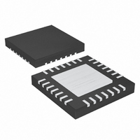
MAX8550ETI+ Maxim Integrated Products, MAX8550ETI+ Datasheet - Page 12

MAX8550ETI+
Manufacturer Part Number
MAX8550ETI+
Description
IC PWR SUP DDR INTEG 28TQFN
Manufacturer
Maxim Integrated Products
Datasheet
1.MAX8550ETIT.pdf
(29 pages)
Specifications of MAX8550ETI+
Applications
Controller, DDR
Voltage - Input
2 ~ 28 V
Number Of Outputs
2
Voltage - Output
1.8V, 2.5V, 0.7 ~ 5.5 V
Operating Temperature
-40°C ~ 85°C
Mounting Type
Surface Mount
Package / Case
28-TQFN Exposed Pad
Output Voltage
0.7 V to 5.5 V, 1.8 V, 2.5 V
Output Current
20 A
Input Voltage
2 V to 28 V
Mounting Style
SMD/SMT
Maximum Operating Temperature
+ 85 C
Minimum Operating Temperature
- 40 C
Lead Free Status / RoHS Status
Lead free / RoHS Compliant
Integrated DDR Power-Supply Solutions for
Desktops, Notebooks, and Graphic Cards
The MAX8550/MAX8551 combine a synchronous-buck
PWM controller, an LDO linear regulator, and a 10mA ref-
erence output buffer. The buck controller drives two exter-
nal N-channel MOSFETs to deliver load currents up to
12A and generate voltages down to 0.7V from a +2V to
+28V input. The LDO linear regulator can sink and source
up to 1.5A continuous and 3A peak current with relatively
fast response. These features make the MAX8550/
MAX8551 ideally suited for DDR memory applications.
The MAX8550/MAX8551 buck regulator is equipped
with a fixed switching frequency of up to 600kHz using
Maxim’s proprietary constant on-time Quick-PWM
architecture. This control scheme handles wide
input/output voltage ratios with ease, and provides
100ns “instant-on” response to load transients, while
maintaining high efficiency with relatively constant
switching frequency.
The buck controller, LDO, and a reference output
buffer are provided with independent current limits.
Lossless foldback current limit in the buck regulator is
achieved by monitoring the drain-to-source voltage
drop of the low-side FET. The ILIM input is used to
adjust this current limit. Overvoltage protection, if
selected, is achieved by latching the low-side synchro-
nous FET on and the high-side FET off when the output
voltage is over 116% of its set output. It also features
an optional undervoltage protection by latching the
MOSFET drivers to the OFF state during an overcurrent
condition, when the output voltage is lower than 70% of
the regulated output. This helps minimize power dissi-
pation during a short-circuit condition.
The current limit in the LDO and buffered reference out-
put buffer is ±5A and ±40mA, respectively, and neither
have the over- or undervoltage protection. When the
current limit in either output is reached, the output no
longer regulates the voltage, but regulates the current
to the value of the current limit.
The MAX8550/MAX8551 require an external +5V bias
supply in addition to the input voltage (V
bias supply external to the IC improves the efficiency
and eliminates the cost associated with the +5V linear
regulator that would otherwise be needed to supply the
PWM circuit and the gate drivers. If stand-alone capabili-
ty is needed, then the +5V supply can be generated with
an external linear regulator such as the MAX1615. V
AV
source is a fixed +4.5V to +5.5V supply.
12
DD
______________________________________________________________________________________
, and IN can be connected together if the input
+5V Bias Supply (V
Detailed Description
DD
IN
). Keeping the
and AV
DD
DD
)
,
V
drivers, and AV
the IC. The current from the AV
supply must supply the current for the IC and the gate
drive for the MOSFETs. This maximum current can be
estimated as:
where I
into V
charges of MOSFETs Q1 and Q2 (at V
Typical Applications Circuit, and f
frequency.
The Quick-PWM control architecture is a pseudo-fixed-
frequency, constant on-time, current-mode regulator
with voltage feed-forward (Figure 1). This architecture
relies on the output filter capacitor’s ESR to act as a
current-sense resistor, so the output ripple voltage pro-
vides the PWM ramp signal. The control algorithm is
simple: the high-side switch on-time is determined
solely by a one-shot whose pulse width is inversely pro-
portional to input voltage and directly proportional to
the output voltage. Another one-shot sets a minimum
off-time of 300ns (typ). The on-time one-shot is trig-
gered if the error comparator is low, the low-side switch
current is below the valley current-limit threshold, and
the minimum off-time one-shot has timed out.
The heart of the PWM core is the one-shot that sets the
high-side switch on-time. This fast, low-jitter, adjustable
one-shot includes circuitry that varies the on-time in
response to input and output voltages. The high-side
switch on-time is inversely proportional to the input volt-
age (V
where K (the switching period) is set by the TON input
connection (Table 1) and R
tance of the synchronous rectifier (Q2) in the Typical
Applications Circuit (Figure 8). This algorithm results in
a nearly constant switching frequency despite the lack
of a fixed-frequency clock generator. The benefits of a
constant switching frequency are twofold:
1) The frequency can be selected to avoid noise-sensi-
DD
tive regions such as the 455kHz IF band.
is the supply input for the buck regulator’s MOSFET
I
BIAS
DD
t
IN
ON
Free-Running Constant-On-Time PWM
VDD
) and is proportional to the output voltage:
and AV
=
=
+ I
I
K
VDD
AVDD
DD
×
DD
(
+
V
supplies the power for the rest of
OUT
, Q
are the quiescent supply currents
I
AVDD
G1
On-Time One-Shot (TON)
+
and Q
I
+
LOAD
DS(ON)Q2
f
SW
V
IN
G2
×
DD
×
SW
(
Q
R
are the total gate
G
DS ON Q
and V
is the switching
1
GS
is the on-resis-
(
+
= 5V) in the
Q
)
DD
G
2
2
)
)
power


