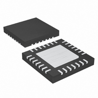
MAX8550ETI+ Maxim Integrated Products, MAX8550ETI+ Datasheet - Page 21

MAX8550ETI+
Manufacturer Part Number
MAX8550ETI+
Description
IC PWR SUP DDR INTEG 28TQFN
Manufacturer
Maxim Integrated Products
Datasheet
1.MAX8550ETIT.pdf
(29 pages)
Specifications of MAX8550ETI+
Applications
Controller, DDR
Voltage - Input
2 ~ 28 V
Number Of Outputs
2
Voltage - Output
1.8V, 2.5V, 0.7 ~ 5.5 V
Operating Temperature
-40°C ~ 85°C
Mounting Type
Surface Mount
Package / Case
28-TQFN Exposed Pad
Output Voltage
0.7 V to 5.5 V, 1.8 V, 2.5 V
Output Current
20 A
Input Voltage
2 V to 28 V
Mounting Style
SMD/SMT
Maximum Operating Temperature
+ 85 C
Minimum Operating Temperature
- 40 C
Lead Free Status / RoHS Status
Lead free / RoHS Compliant
The VTTR buffer is a scaled-down version of the VTT
regulator, with much smaller output transconductance.
Its compensation cap can therefore be smaller, and its
ESR larger, than what is required for its larger counter-
part. For typical applications requiring load current up
to ±20mA, a ceramic cap with a minimum value of 1µF
is recommended (R
between VTTR and the analog ground plane.
Both the VTT and VTTR output stages are powered
from the same VTTI input. Their output voltages are ref-
erenced to the same REFIN input. The value of the VTTI
bypass capacitor is chosen to limit the amount of rip-
ple/noise at VTTI, or the amount of voltage dip during a
load transient. Typically VTTI is connected to the output
of the buck regulator, which already has a large bulk
capacitor. Nevertheless, a ceramic capacitor of at least
10µF must be used and must be added and placed as
close as possible to the VTTI pin. This value must be
increased with larger load current, or if the trace from
the VTTI pin to the power source is long and has signifi-
cant impedance. Furthermore, to prevent undesirable
VTTI bounce from coupling back to the REFIN input
and possibly causing instability in the loop, the REFIN
pin should ideally tap its signal from a separate low-
impedance DC source rather than directly from the
VTTI input. If the latter is unavoidable, increase the
amount of bypass capacitance at the VTTI input and
add additional bypass at the REFIN pin.
The MAX8550/MAX8551 drive external, logic-level, N-
channel MOSFETs as the circuit-switch elements. The
key selection parameters:
On-resistance (R
Maximum drain-to-source voltage (V
at least 20% higher than input supply rail at the high-
side MOSFET’s drain.
Gate charges (Q
Choose MOSFETs with rated R
For a good compromise between efficiency and cost,
choose the high-side MOSFET that has a conduction
loss equal to its switching loss at nominal input voltage
and maximum output current (see below). For the low-
side MOSFET, make sure that it does not spuriously
turn on because of dV/dt caused by the high-side
MOSFET turning on, as this results in shoot-through
current degrading efficiency. MOSFETs with a lower
Q
GD
VTTR Output Capacitor Selection (LDO)
to Q
VTTI Input Capacitor Selection (LDO)
GS
Integrated DDR Power-Supply Solutions for
ratio have higher immunity to dV/dt.
Desktops, Notebooks, and Graphic Cards
G
DS(ON)
______________________________________________________________________________________
, Q
GD
ESR
MOSFET Selection (Buck)
, Q
): the lower, the better.
< 0.3Ω). Connect this cap
GS
): the lower the better.
DS(ON)
DSS
at V
): should be
GS
= 4.5V.
For proper thermal-management design, calculate the
power dissipation at the desired maximum operating
junction temperature, maximum output current, and
worst-case input voltage. For the low-side MOSFET, the
worst case is at V
the worst case could be at either V
The high-side MOSFET and low-side MOSFET have dif-
ferent loss components due to the circuit operation.
The low-side MOSFET operates as a zero-voltage
switch; therefore, major losses are:
• The channel-conduction loss (P
• The body-diode conduction loss (P
• The gate-drive loss (P
Use R
where V
the dead time (≈30ns), and f
quency. Because of the zero-voltage switch operation,
the low-side MOSFET gate-drive loss occurs as a result
of charging and discharging the input capacitance,
(C
gate-driver’s pullup and pulldown resistance, R
(≈1Ω), and the internal gate resistance (R
MOSFET (≈2Ω). The drive power dissipated is given by:
switch and has the following major losses:
• The channel-conduction loss (P
• The VI overlapping switching loss (P
• The drive loss (P
(The high-side MOSFET does not have body-diode
conduction loss because the diode never conducts
current):
Use R
The high-side MOSFET operates as a duty-cycle control
ISS
P
LSDR
). This loss is distributed among the average DL
P
DS(ON)
DS(ON)
LSCC
P
F
P
LSDC
HSCC
is the body-diode forward-voltage drop, t
=
C
=
at T
at T
ISS
⎛
⎜
⎝
=
=
1
J(MAX)
J(MAX)
-
2
IN(MAX)
×
HSDR
V
I
LOAD
OUT
V
V
V
IN
OUT
V
GS
IN
:
:
LSDR
)
2
. For the high-side MOSFET,
×
⎞
⎟ ×
⎠
×
×
I
LOAD
):
V
f
F
SW
SW
I
LOAD
×
LSCC
HSCC
2
is the switching fre-
×
IN(MIN)
t
×
DT
2
LSDC
R
HSSW
×
)
GATE
R
)
DS ON
×
R
R
GATE
)
DS ON
GATE
(
f
or V
SW
)
+
(
)
R
IN(MAX)
) of the
DL
)
DT
DL
21
is
.


