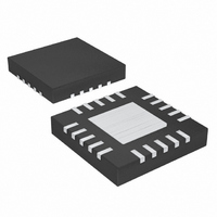
MAX1515ETG+T Maxim Integrated Products, MAX1515ETG+T Datasheet - Page 17

MAX1515ETG+T
Manufacturer Part Number
MAX1515ETG+T
Description
IC REG DDR LV 24-TQFN
Manufacturer
Maxim Integrated Products
Datasheet
1.MAX1515ETG.pdf
(24 pages)
Specifications of MAX1515ETG+T
Applications
Converter, DDR
Voltage - Input
1.3 ~ 3.6 V
Number Of Outputs
2
Voltage - Output
0.5 ~ 2.7 V
Operating Temperature
-40°C ~ 85°C
Mounting Type
Surface Mount
Package / Case
24-TQFN Exposed Pad
Lead Free Status / RoHS Status
Lead free / RoHS Compliant
resistive divider between REF and ground (Figure 5).
Regulation is maintained for adjustable output voltages
when V
the equation:
where V
The preset output voltages use an internally trimmed
resistor-divider network that sets the output voltage to
the correct level when REFIN is connected to REF.
Connecting REFIN to other voltage levels while using
the preset voltage modes results in a ratiometrically
scaled output voltage.
In DDR mode (MODE = V
FB to the voltage set at REFIN. For DDR applications,
the termination supply must track to exactly half the
memory supply voltage. Figure 1 shows the MAX1515
configured for DDR applications.
A unity-gain amplifier provides a buffered output for the
reference input (V
transconductance amplifier must be compensated with
a 0.47µF or greater ceramic capacitor. Larger capaci-
tor values decrease the amplifier’s bandwidth, thereby
increasing the response time to dynamic input-voltage
changes. The buffer allows this dynamic reference to
remain within ±20mV of the input voltage (V
when loaded with ±5mA. The input voltage range of the
amplifier is 0.5V to 1.5V. The reference buffer shuts
down when MODE = GND.
PGOOD is the open-drain output for a window compara-
tor that continuously monitors the output. PGOOD is
actively held low in shutdown and during soft-start. After
soft-start terminates, PGOOD becomes high impedance
as long as the respective output voltage is within ±10%
of the nominal regulation voltage. When the output volt-
age drops 10% below or rises 10% above the nominal
regulation voltage, the MAX1515 pulls the power-good
output (PGOOD) low by turning on the MOSFET (Figure
2). For logic-level output voltages, connect an external
pullup resistor between PGOOD and V
resistor works well in most applications.
The MAX1515 features a thermal fault-protection circuit.
When the junction temperature rises above +165°C, a
thermal sensor shuts down the MAX1515 regardless of
FB
REF
= V
= 1.1V.
REFIN
V
FB
Power-Good Output (PGOOD)
______________________________________________________________________________________
. Use 100kΩ for R
=
Reference Buffer (REFOUT)
REFIN
V
REF
Output Voltage in DDR Mode
) when MODE = V
CC
⎛
⎜
⎝
R
), the MAX1515 regulates
A
Thermal Shutdown
R
+
B
R
B
B
⎞
⎟
⎠
. R
CC
A
REFIN
Low-Voltage, Internal Switch,
is given by
. A 100kΩ
CC
) even
. This
Step-Down/DDR Regulator
V
temperature cools to +150°C.
Junction-to-ambient thermal resistance, θ
dependent on the amount of copper area connected to
the exposed backside pad. Airflow over the board sig-
nificantly reduces θ
distribute the copper area connected at the IC among
the high-current pins. Refer to the Maxim website
(www.maxim-ic.com) for QFN thermal considerations.
Power dissipation in the MAX1515 is dominated by
conduction losses in the two internal power switches.
Power dissipation due to supply current in the control
section and average current used to charge and dis-
charge the gate capacitance of the internal switches
(i.e., switching losses—PSL) is approximately:
Figure 4. Sink-Mode Waveforms
Figure 5. Setting V OUT with a Resistive Voltage-Divider at REFIN
INDUCTOR
SHDN
CURRENT
CURRENT
VOLTAGE
VOLTAGE
OUTPUT
LOAD
LX
R
R
A
B
. The MAX1515 is reactivated after the junction
t
OFF
PSL = C x V
REF
REFIN
MODE
FBSEL0
FBSEL1
JA
. For heatsinking purposes, evenly
MAX1515
PGND
IN
GND
Thermal Resistance
LX
FB
2
Power Dissipation
x f
SW
L
JA
, is highly
C
V
OUT
OUT
0
-2A
0
-2A
V
V
V
GND
REFIN
IN
OUT
17


