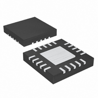
MAX1515ETG+T Maxim Integrated Products, MAX1515ETG+T Datasheet - Page 15

MAX1515ETG+T
Manufacturer Part Number
MAX1515ETG+T
Description
IC REG DDR LV 24-TQFN
Manufacturer
Maxim Integrated Products
Datasheet
1.MAX1515ETG.pdf
(24 pages)
Specifications of MAX1515ETG+T
Applications
Converter, DDR
Voltage - Input
1.3 ~ 3.6 V
Number Of Outputs
2
Voltage - Output
0.5 ~ 2.7 V
Operating Temperature
-40°C ~ 85°C
Mounting Type
Surface Mount
Package / Case
24-TQFN Exposed Pad
Lead Free Status / RoHS Status
Lead free / RoHS Compliant
The MAX1515 can sustain a constant short circuit or
overload. Under a source-mode short-circuit or over-
load condition, when V
MAX1515 uses an extended off-time to control the cur-
rent. Operation during a short circuit or overload is sim-
ilar to forced-PWM mode except the off-time is 4 x t
At the end of each off-time, the high-side NMOS switch
turns on and remains on until the output is in regulation
or the current through the switch increases to the maxi-
mum current limit. When the high-side NMOS switch
turns off, it remains off for four times the programmed
off-time (t
switch turns on. Since either NMOS switch is always on,
the inductor current is continuous. The RMS inductor
current during a short circuit remains below the maxi-
mum current-limit threshold. The MAX1515 operates
using the extended off-time until the short circuit or
overload is removed and V
Prolonged short circuit or overload can result in thermal
shutdown.
Three signals are added together at the input of the
summing comparator (Figure 2): an output-voltage
error signal relative to the reference voltage, an inte-
grated output-voltage error-correction signal, and the
sensed high-side NMOS switch current. The integrated
error signal is provided by a transconductance amplifi-
er with an external capacitor at COMP. This integrator
provides high DC accuracy without the need for a high-
gain amplifier. Connecting a capacitor at COMP modi-
fies the overall loop response (see the Integrator
Amplifier section).
The MAX1515 includes an internal transconductance
amplifier that improves the output DC accuracy.
Figure 3. Soft-Start Current Limit
I
LIMIT
V
SHDN
SS
(V)
(A)
OFF
Short-Circuit/Overload Protection
), and the low-side NMOS synchronous
0.7V
______________________________________________________________________________________
FB
Summing Comparator
Integrator Amplifier
< 0.3 x V
FB
> 0.3 x V
TARGET
Low-Voltage, Internal Switch,
TARGET
1.8V
I
LIMIT_P
, the
OFF.
Step-Down/DDR Regulator
.
A capacitor, C
the transconductance amplifier. For stability, choose
C
Use MODE to configure the MAX1515 for DDR mode
(MODE = V
DDR mode, the MAX1515 can sink current even while
SKIP is low (see the Pulse Skipping (Source Mode) and
Pulse Skipping (Sink Mode) sections). Also, DDR mode
enables the REFOUT buffer, providing a buffered out-
put of the REFIN voltage. In non-DDR mode, the
MAX1515 can only source current when SKIP is low.
The REFOUT buffer is also disabled in non-DDR mode.
The MAX1515 includes a pulse-skipping mode that
reduces current consumption during light loads. To con-
figure the MAX1515 for pulse-skipping mode, connect
SKIP to GND. Forced-PWM mode keeps the switching
frequency relatively constant and is desirable in appli-
cations that must always keep the frequency of con-
ducted and radiated emissions in a narrow band. Visit
Maxim’s website (www.maxim-ic.com) for more informa-
tion on how to control electromagnetic interference
(EMI). Pulse-skipping mode has a dynamic switching
frequency under light loads and is desirable in applica-
tions that require high efficiency at light loads.
Connect SKIP to V
in low-noise, constant-off-time PWM mode. Constant
off-time PWM architecture provides a relatively constant
switching frequency (see the Frequency Variation with
Output Current section). A single resistor (R
the high-side NMOS power-switch off-time that results
in a switching frequency up to 1MHz, allowing perfor-
mance trade-offs in efficiency, switching noise, compo-
nent size, and cost.
Forced-PWM mode regulates the output voltage by
increasing the high-side NMOS switch on-time to
increase the amount of energy transferred to the load
per cycle. At the end of each off-time, the high-side
NMOS switch turns on and remains on until the output is
in regulation or the current through the switch reaches
the 4.2A current limit. When the high-side NMOS switch
turns off, it remains off for the programmed off-time
(t
turns on. The low-side NMOS switch remains on until the
end of t
PWM mode, the inductor current is continuous.
OFF
COMP
), and the low-side NMOS synchronous switch
= 470pF.
OFF
. Since either NMOS switch is always on in
CC
COMP
) or non-DDR mode (MODE = GND). In
CC
Light-Load Operation (
Modes of Operation (MODE)
, from COMP to V
to force the MAX1515 to operate
Forced-PWM Mode
CC
compensates
TOFF
SKIP )
) sets
15


