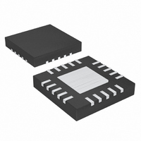
MAX1515ETG+T Maxim Integrated Products, MAX1515ETG+T Datasheet - Page 16

MAX1515ETG+T
Manufacturer Part Number
MAX1515ETG+T
Description
IC REG DDR LV 24-TQFN
Manufacturer
Maxim Integrated Products
Datasheet
1.MAX1515ETG.pdf
(24 pages)
Specifications of MAX1515ETG+T
Applications
Converter, DDR
Voltage - Input
1.3 ~ 3.6 V
Number Of Outputs
2
Voltage - Output
0.5 ~ 2.7 V
Operating Temperature
-40°C ~ 85°C
Mounting Type
Surface Mount
Package / Case
24-TQFN Exposed Pad
Lead Free Status / RoHS Status
Lead free / RoHS Compliant
Table 3. Modes of Operation
Low-Voltage, Internal Switch,
Step-Down/DDR Regulator
X = Don’t care.
Connect SKIP to GND to allow the MAX1515 to auto-
matically switch between high-efficiency pulse-skipping
mode under light loads and PWM mode under heavy
loads. The transition from PWM mode to pulse-skipping
mode occurs when the load current is half the pulse-
skipping mode current threshold (800mA typ).
In pulse-skipping mode, the switching frequency is
reduced to increase efficiency. The inductor current is
discontinuous in this mode, and the MAX1515 only initi-
ates an LX switching cycle when V
V
turns on and remains on until output is in regulation and
the current through the switch increases to the positive
pulse-skipping-mode current threshold (I
800mA. When the high-side NMOS switch turns off, the
low-side NMOS synchronous switch turns on and
remains on until the current through the switch decreas-
es to the zero-cross-current threshold of 200mA.
When pulse-skipping operation is selected (SKIP =
GND) while in DDR mode (MODE = V
MAX1515’s source/sink controller switches operating
modes when the output voltage crosses either hys-
teretic sink/source thresholds (V
pulse-skipping source mode, the MAX1515 regulates
the valley of the output ripple voltage (see the Pulse
Skipping (Source Mode) section). When the output volt-
age rises above the sink-mode threshold, the MAX1515
enters sink mode. The MAX1515 begins each sink-
mode cycle by turning on the low-side NMOS. The low-
side NMOS remains on until the off-time (t
low-side NMOS turns off, the high-side NMOS turns on
16
FB
SHDN
High
High
High
High
Low
Low
______________________________________________________________________________________
falls below V
MODE
High
High
High
Low
Low
Low
PIN
REFIN
Pulse Skipping (Source Mode)
, the high-side NMOS switch
Pulse Skipping (Sink Mode)
SKIP
High
High
Low
Low
X
X
FB
REFIN
Off, High-Z
Off, High-Z
Off, High-Z
REFOUT
BUFFER
< V
On
On
On
OFF
REFIN
±25mV). In
SKIP_P
). After the
CC
. When
FB regulates to preset voltage or 0.5V.
FB regulates to preset voltage or 0.5V.
), the
) of
FB regulates to REFIN.
FB regulates to REFIN.
REGULATOR MODE
On, non-DDR mode.
On, non-DDR mode.
On, DDR mode.
On, DDR mode.
STEP-DOWN
Table 4. Output-Voltage Programming
and remains on until the current through the switch
reaches the zero-cross-current threshold of -350mA. As
long as the output voltage remains below the feedback
threshold, the controller remains in the high-impedance
state. Under light-load conditions, this allows the sink-
mode controller to automatically skip pulses. Under
heavy-load conditions, the output voltage remains
above the feedback threshold, forcing the sink-mode
controller to emulate typical forced-PWM operation.
The pulse-skipping current threshold allows the sink-
mode control scheme to automatically switch between
pulse-skipping PFM and nonskipping PWM operation.
This mechanism forces the boundary between continu-
ous and discontinuous inductor-current operation to be
half the negative pulse-skipping current threshold.
In non-DDR mode (MODE = GND and V
the output of the MAX1515 is selectable between one
of three preset output voltages: 2.5V, 1.8V, and 1.5V.
For a preset output voltage, connect FB to the output
voltage and connect FBSEL0 and FBSEL1 as indicated
in Table 4. For an adjustable output voltage, connect
FBSEL0 and FBSEL1 to GND and connect REFIN to a
Off
Off
FBSEL0
GND
GND
V
V
CC
CC
Output Voltage in Non-DDR Mode
FBSEL1
GND
GND
V
V
CC
CC
REGULATOR CURRENT
Pulse-skipping mode.
Pulse-skipping mode.
Forced-PWM mode.
Forced-PWM mode.
STEP-DOWN
Source only.
Source/sink.
Source/sink.
Source/sink.
Off
Off
V
REFIN
VOLTAGE
Adjustable
FB
OUTPUT
= V
1.5V
1.8V
2.5V
= V
REFIN
REF
),


