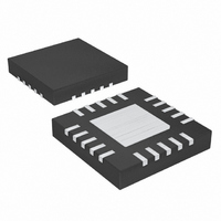
MAX1515ETG+T Maxim Integrated Products, MAX1515ETG+T Datasheet - Page 11

MAX1515ETG+T
Manufacturer Part Number
MAX1515ETG+T
Description
IC REG DDR LV 24-TQFN
Manufacturer
Maxim Integrated Products
Datasheet
1.MAX1515ETG.pdf
(24 pages)
Specifications of MAX1515ETG+T
Applications
Converter, DDR
Voltage - Input
1.3 ~ 3.6 V
Number Of Outputs
2
Voltage - Output
0.5 ~ 2.7 V
Operating Temperature
-40°C ~ 85°C
Mounting Type
Surface Mount
Package / Case
24-TQFN Exposed Pad
Lead Free Status / RoHS Status
Lead free / RoHS Compliant
PIN
1, 2
10
11
12
13
14
15
16
17
3
4
5
6
7
8
9
REFOUT
PGOOD
FBSEL0
NAME
COMP
MODE
PGND
REFIN
SHDN
TOFF
GND
V
V
REF
SS
FB
______________________________________________________________________________________
IC
DD
CC
Power Ground. Internal connection to the source of the internal synchronous-rectifier switch. Connect
both PGND pins together.
Internally Connected Pin. Connect to PGND.
Supply Input for the Low-Side Gate Drive and REFOUT Buffer. Connect to the system supply voltage,
+3.0V to +3.6V. Bypass to PGND with a 1µF (min) ceramic capacitor. V
drivers and the REFOUT buffer.
REFIN Buffered Output. REFOUT provides a buffered output voltage of REFIN when MODE = V
Bypass to GND with a 0.47µF ceramic capacitor. REFOUT is disabled when MODE = GND.
Soft-Start. Connect a capacitor from SS to GND to limit the inrush current during startup.
Power-Good Open-Drain Output. PGOOD is low when the output voltage is more than 10% above or
below the normal regulation point. PGOOD is high impedance when the output is in regulation.
PGOOD is low in shutdown.
Off-Time Select Input. Connect a resistor from TOFF to GND to adjust the off-time.
Feedback Input.
In DDR mode (MODE = V
In non-DDR mode (MODE = GND), connect directly to the output for preset voltage operation or to a
resistive voltage-divider for adjustable-mode operation.
Integrator Compensation. Connect a 470pF capacitor from COMP to V
compensation.
Analog Supply Input. Connect to the system supply voltage, +3.0V to +3.6V, with a series 10Ω
resistor. Bypass to GND with a 1µF (min) ceramic capacitor.
Analog Ground. Connect exposed backside pad to GND.
+1.1V Reference Voltage Output. Bypass to GND with a 1.0µF bypass capacitor. Can supply 50µA
for external loads. Reference turns off in shutdown.
External Reference Input. In DDR mode (MODE = V
In non-DDR mode (MODE = GND), connect REFIN to REF.
Shutdown Control. Low disables the switching regulator. SHDN and MODE select the operational
mode of the MAX1515.
SHDN
Low
Low
High
High
Mode-Select Pin. Mode sets the regulator into DDR mode or non-DDR operation mode, and controls
the REFOUT buffer. When MODE = V
MODE = GND, MAX1515 is set in non-DDR mode and REFOUT is disabled. See the Modes of
Operation (MODE) section.
Used with FBSEL1 to set the output voltage of the step-down regulator when MODE = GND.
Connect to GND if MODE = V
MODE
Low
High
Low
High
Low-Voltage, Internal Switch,
Description
Step-down regulator and REFOUT OFF
Step-down regulator OFF, REFOUT active
Step-down regulator ON, non-DDR mode, REFOUT OFF
Step-down regulator ON, DDR mode, REFOUT active
CC
), FB regulates to the voltage at REFIN.
CC
Step-Down/DDR Regulator
.
CC
, MAX1515 is set in DDR mode and REFOUT is active. When
FUNCTION
CC
), REFIN sets the voltage that FB regulates to.
CC
DD
for integrator
supplies power to the
Pin Description
CC
.
11


