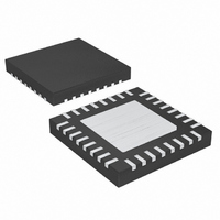
MAX1997ETJ+T Maxim Integrated Products, MAX1997ETJ+T Datasheet - Page 26

MAX1997ETJ+T
Manufacturer Part Number
MAX1997ETJ+T
Description
IC PWR SUPPLY TFT LCD 32TQFN
Manufacturer
Maxim Integrated Products
Datasheet
1.MAX1997ETJ.pdf
(31 pages)
Specifications of MAX1997ETJ+T
Applications
Controller, TFT, LCD
Voltage - Input
2.7 ~ 5.5 V
Number Of Outputs
5
Voltage - Output
2.7 ~ 13 V
Operating Temperature
0°C ~ 85°C
Mounting Type
Surface Mount
Package / Case
32-TQFN Exposed Pad
Lead Free Status / RoHS Status
Lead free / RoHS Compliant
Quintuple/Triple-Output TFT LCD Power Supplies
with Fault Protection and VCOM Buffer
Increasing the flying capacitor (C
output current capability. Increasing the capacitance
indefinitely has a negligible effect on output current
capability because the internal switch resistance and
the diode impedance limit the source impedance. A
0.1µF ceramic capacitor works well in most low-current
applications. The flying capacitor’s voltage rating must
exceed the following:
where N is the stage number in which the flying capaci-
tor appears, and V
example, the two-stage positive charge pump in the
typical application circuit (Figure 1) where V
contains two flying capacitors. The flying capacitor in
the first stage (C25) requires a voltage rating greater
than 9V. The flying capacitor in the second stage (C24)
requires a voltage rating greater than 18V.
Increasing the output capacitance or decreasing the
ESR reduces the output ripple voltage and the peak-to-
peak transient voltage. With ceramic capacitors, the
output voltage ripple is dominated by the capacitance
value. Use the following equation to approximate the
required capacitor value:
where V
ripple.
Use Schottky diodes with a current rating equal to or
greater than two times the average charge-pump input
current. If the loaded charge-pump output voltage is
greater than required, some or all of the Schottky
diodes can be replaced with low-cost silicon switching
diodes with an equivalent current rating. The charge-
pump input current is:
where N is the number of charge-pump stages.
Adjust the positive linear-regulator (REG P) output volt-
age by connecting a resistive voltage-divider from
V
(Figure 1). Select R20 in the range of 10kΩ to 30kΩ.
26
G_ON
______________________________________________________________________________________
to GND with the center tap connected to FBP
RIPPLE
C
is the peak-to-peak value of the output
OUT
I
CP
Linear-Regulator Controllers
MAIN
V
_
CX
≥
IN
Charge-Pump Output Capacitor
2f
Charge-Pump Rectifier Diodes
> N
= I
OSC RIPPLE
is the main output voltage. For
I
CP
LOAD
✕
V
Output Voltage Selection
_
V
OUT
MAIN
X
) value increases the
✕
Flying Capacitors
N
MAIN
= 9V
Calculate R19 with the following equation:
where V
The output voltages of linear regulators REG 1 and
REG 2 can be similarly adjusted.
Adjust the negative linear-regulator (REG N) output
voltage by connecting a resistive voltage-divider from
V
(Figure 1). Select R17 in the range of 10kΩ to 30kΩ.
Calculate R16 with the following equation:
where V
up to 75µA, using a resistor greater than 17kΩ for R17
leaves at least 10µA for other uses.
The pass transistor must meet specifications for current
gain (β), input capacitance, collector-emitter saturation
voltage, and power dissipation. The transistor’s current
gain limits the guaranteed maximum output current to:
where I
rent, V
and R
transistor’s base and emitter. Furthermore, the transis-
tor’s current gain increases the linear regulator’s DC
loop gain (see the Stability Requirements section), so
excessive gain destabilizes the output. Therefore, tran-
sistors with current gain over 100 at the maximum out-
put current can be difficult to stabilize and are not
recommended. The transistor’s input capacitance and
input resistance also create a second pole, which
could be low enough to make the output unstable when
heavily loaded.
The transistor’s saturation voltage at the maximum out-
put current determines the minimum input-to-output
voltage differential that the linear regulator supports.
Alternatively, the package’s power dissipation could
limit the usable maximum input-to-output voltage differ-
ential. The maximum power dissipation capability of the
transistor’s package and mounting must exceed the
actual power dissipation in the device. The power dissi-
pation equals the maximum load current times the max-
imum input-to-output voltage differential:
P = I
G_OFF
LOAD(MAX)
R16 = R17 [(V
BE
BE
DRV
FBP
FBN
I
to REF with the center tap connected to FBN
LOAD(MAX)
is the pullup resistor connected between the
is the base-to-emitter voltage of the transistor,
is the minimum guaranteed base drive cur-
R19 = R20 [(V
= 1.25V.
= 125mV, V
(V
LDOIN
FBN
=
I
DRV
- V
- V
REF
G_ON
G_OFF
LDOOUT
−
Pass Transistor Selection
= 1.25V. REF can source
R
V
BE
BE
/ V
) / (V
FBP
β
) = I
MIN
REF
) - 1]
LOAD(MAX)
- V
FBN
)]
V
CE


