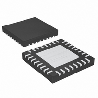
MAX1997ETJ+T Maxim Integrated Products, MAX1997ETJ+T Datasheet - Page 10

MAX1997ETJ+T
Manufacturer Part Number
MAX1997ETJ+T
Description
IC PWR SUPPLY TFT LCD 32TQFN
Manufacturer
Maxim Integrated Products
Datasheet
1.MAX1997ETJ.pdf
(31 pages)
Specifications of MAX1997ETJ+T
Applications
Controller, TFT, LCD
Voltage - Input
2.7 ~ 5.5 V
Number Of Outputs
5
Voltage - Output
2.7 ~ 13 V
Operating Temperature
0°C ~ 85°C
Mounting Type
Surface Mount
Package / Case
32-TQFN Exposed Pad
Lead Free Status / RoHS Status
Lead free / RoHS Compliant
Quintuple/Triple-Output TFT LCD Power Supplies
with Fault Protection and VCOM Buffer
(Circuit of Figure 1, V
unless otherwise noted.)
10
MAX1997
2.2
2.1
2.0
1.9
1.8
1.7
______________________________________________________________________________________
1
2
3
C
D
A
B
2.5
OVERCURRENT PROTECTION RESPONSE
LX CURRENT LIMIT vs. INPUT VOLTAGE
A: V
B: V
C: V
D: V
T
T
T
A
A
TO OVERLOAD DURING STARTUP
MAIN
GATE
A
PIN
G_ON
G_OFF
= +25°C
= +85°C
= -40°C
3.0
, 5V/div
, 5V/div
, 10V/div
MAX1998
, 10V/div
INPUT VOLTAGE (V)
3.5
—
—
1
20ms/div
4.0
IN
= 3.3V, V
TGNDB
NAME
4.5
PGND
DRV1
5.0
MAX1997 toc20
MAIN
Internal Connection. Connect this pin to ground. Do not leave this pin floating.
Power Ground. PGND is the source of the N-channel power MOSFET. Connect PGND to the
star ground at the device’s backside pad.
Logic Linear-Regulator (REG 1) Base Drive. Open drain of an internal N-channel MOSFET.
Connect DRV1 to the base of an external PNP linear regulator pass transistor. (See the Pass
Transistor Selection section).
5.5
10V
5V
0
5V
0
20V
10V
0
-10V
= 9V, V
10
8
6
4
2
0
TO OVERLOAD DURING NORMAL OPERATION
C
D
A
B
Typical Operating Characteristics (continued)
-40
OVERCURRENT PROTECTION RESPONSE
A: V
B: V
C: V
D: V
VCOM BUFFER TRANSCONDUCTANCE
G_ON
MAIN
GATE
G_ON
G_OFF
-20
, 5V/div
, 5V/div
, 10V/div
, 10V/div
= 20V, V
vs. TEMPERATURE
0
TEMPERATURE (°C)
LARGE-SIGNAL
TRANSCONDUCTANCE
SMALL-SIGNAL
TRANSCONDUCTANCE
20
20ms/div
G_OFF
40
60
= -7V, V
MAX1997 toc21
80
FUNCTION
100
LOGIC
10V
5V
0
5V
0
20V
10V
0
-10V
= 2.5V, V
1.250
1.249
1.248
1.247
1.246
C
A
B
A: LOAD CURRENT, 1A/div
B: V
C: V
VCOM LOAD TRANSIENT RESPONSE
OUTB
1
X
, 20V/div
(CIRCUIT OF PAGE 6, NOTE 4)
= 3.6V, 200mV/div, AC-COUPLED
GAMMA
Pin Description
REFERENCE VOLTAGE
vs. LOAD CURRENT
LOAD CURRENT (µA)
4µs/div
= 8.6V, T
10
A
MAX1997 toc25
= +25°C,
1A
0
-1A
3.8V
3.6V
3.4V
20V
0
-20V
100


