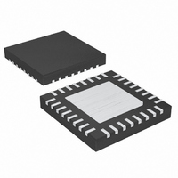
MAX1997ETJ+T Maxim Integrated Products, MAX1997ETJ+T Datasheet - Page 23

MAX1997ETJ+T
Manufacturer Part Number
MAX1997ETJ+T
Description
IC PWR SUPPLY TFT LCD 32TQFN
Manufacturer
Maxim Integrated Products
Datasheet
1.MAX1997ETJ.pdf
(31 pages)
Specifications of MAX1997ETJ+T
Applications
Controller, TFT, LCD
Voltage - Input
2.7 ~ 5.5 V
Number Of Outputs
5
Voltage - Output
2.7 ~ 13 V
Operating Temperature
0°C ~ 85°C
Mounting Type
Surface Mount
Package / Case
32-TQFN Exposed Pad
Lead Free Status / RoHS Status
Lead free / RoHS Compliant
The frequencies of the zero and pole for the lead com-
pensation are:
At high frequencies, R9 is effectively in parallel with R7,
determining the amount of added high-frequency gain. If
R9 is very large, there is no added gain and as R9
approaches zero, the added gain approaches the inverse
of the feedback divider’s attenuation. A typical value for
R9 is greater than half of R7. The value of C9 determines
the frequency placement of the zero and pole. A typical
value of C9 is between 100pF and 10nF. When adding
lead compensation, always check the loop stability by
monitoring the transient response to a pulsed output load.
Adding lag compensation (an RC network from FB to
ground) decreases the loop bandwidth and improves
FB noise immunity. Lag compensation slows the tran-
sient response but can increase stability margin, which
can be needed for particular component choices, a
poor layout, or high values of FB divider resistors (R8
greater than 1.5kΩ).
Lag compensation adds a pole-zero pair, attenuating
gain at higher frequencies and lowering loop band-
width. The frequencies of the pole and zero for lag com-
pensation depend on the feedback divider resistors and
the RC network between FB and GND (Figure 9).
The frequencies of the pole and zero for the lag com-
pensation are:
At high frequencies, R10 is effectively in parallel with
R8, increasing the divider attenuation ratio. If R10 is
very large, the attenuation ratio remains unchanged
and as R10 approaches zero, the attenuation ratio
approaches infinity. A typical value for R10 is greater
than 0.1 times R8. If high-value divider resistors are
used, choose R10 < 1.5kΩ for FB noise immunity. The
value of C10 determines the frequency placement of
the pole and zero. A typical value of C10 is between
100pF and 1000pF.
Quintuple/Triple-Output TFT LCD Power Supplies
f
f
f
f
Z_LEAD
P_LEAD
P_LAG
Z_LAG
______________________________________________________________________________________
=
=
=
=
2
2
2
2
π
π (
with Fault Protection and VCOM Buffer
π
π
R
(
10
R
R
R
10
1
7
9
×
+
+
1
+
C
R
R
R
10
R
R
9
1
7
7
)
1
7
7
)
×
×
×
×
+
C
R
R
R
R
9
8
8
8
8
×
×
C
C
9
10
When adding lag compensation, always check the loop
stability by monitoring the transient response to a
pulsed output load.
The circuit of Figure 1 works well without compensation.
The circuit of Figure 9 uses lag compensation to allow
higher value FB divider resistors, at the expense of
transient response speed, potentially requiring higher
value output capacitors (see Typical Operating
Characteristics). Using one of these two circuits is
recommended.
The digital soft-start of the main step-up regulator limits
the average input current during startup. If even
smoother startup is needed, add a low-frequency lead
compensation network (Figure 9). The improved soft-
start is active only during startup when the output volt-
age rises. Positive changes in the output are
instantaneously coupled to the FB pin through D1 and
feed-forward capacitor C9. This arrangement generates
a smoothly rising output voltage. When the output volt-
age reaches regulation, capacitor C9 charges up
through R9 and diode D1 turns off. If desired, C9 and
R9 can be chosen also to provide some lead compen-
sation in normal operation. In most applications, lead
compensation is not needed, and can be disabled by
making R9 large. With R9 much greater than R7, the
pole and the zero in the compensation network are very
close to one another and cancel out after startup, elimi-
nating the effect of the lead compensation.
The input capacitor (C
drawn from the input supply and reduces noise injec-
tion into the device. A 10µF ceramic capacitor is used
in the standard application circuit (Figure 1) because of
the high source impedance seen in typical lab setups.
Actual applications usually have much lower source
impedance since the step-up regulator often runs
directly from the output of another regulated supply.
Typically, C
in the standard applications circuit. Ensure a low-noise
supply at the IN pin by using adequate C
natively, greater voltage variation can be tolerated on
C
ter (see R1, C1 in Figure 1).
The MAX1997/MAX1998s’ high switching frequency
demands a high-speed rectifier. Schottky diodes are rec-
ommended for most applications because of their fast
recovery time and low forward voltage. In general, a 1A
Schottky diode complements the internal MOSFET well.
IN
if IN is decoupled from C
Using Compensation for Improved Soft-Start
IN
may be reduced below the values used
IN
) reduces the current peaks
IN
using an RC lowpass fil-
Input Capacitor
Rectifier Diode
IN
. Alter-
23


