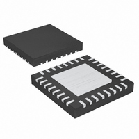
MAX1997ETJ+T Maxim Integrated Products, MAX1997ETJ+T Datasheet - Page 20

MAX1997ETJ+T
Manufacturer Part Number
MAX1997ETJ+T
Description
IC PWR SUPPLY TFT LCD 32TQFN
Manufacturer
Maxim Integrated Products
Datasheet
1.MAX1997ETJ.pdf
(31 pages)
Specifications of MAX1997ETJ+T
Applications
Controller, TFT, LCD
Voltage - Input
2.7 ~ 5.5 V
Number Of Outputs
5
Voltage - Output
2.7 ~ 13 V
Operating Temperature
0°C ~ 85°C
Mounting Type
Surface Mount
Package / Case
32-TQFN Exposed Pad
Lead Free Status / RoHS Status
Lead free / RoHS Compliant
Quintuple/Triple-Output TFT LCD Power Supplies
with Fault Protection and VCOM Buffer
Table 3. Fault Timer Duration
*For MAX1997 only.
**The MAX1998 has PFLT internally connected high.
The high-side overcurrent comparator of the
MAX1997/MAX1998 provides input overcurrent protec-
tion when it is used together with the external P-channel
MOSFET switch P1 (Figure 1). Connect resistive volt-
age-dividers from the source and drain of P1 to GND to
set the overcurrent threshold. The center taps of the
dividers are connected to the overcurrent comparator
inputs (OCN and OCP). See Setting the Input
Overcurrent Threshold section for information on calcu-
lating the resistor values. An overcurrent event acti-
vates the fault-protection circuitry. (See the Fault
Protection section.)
During steady-state operation, if the output of the main
regulator or any of the linear-regulator outputs is below
its respective fault detection threshold, or an input over-
current condition occurs, the MAX1997/MAX1998 acti-
vate an internal fault timer (Figure 8). If any condition or
the combination of conditions indicates a continuous
fault for the fault timer duration (see Table 3), the
MAX1997/MAX1998 set the fault latch, shutting down
all the outputs except the reference and the oscillator.
The fault detection circuit is disabled during the soft-
start time of each regulator. Once the fault condition is
removed, toggle SHDN (below 0.4V) or cycle the input
voltage (below 2.2V) to clear the fault latch and reacti-
vate the device.
The thermal shutdown feature limits total power dissipa-
tion in the MAX1997/MAX1998. If the junction tempera-
ture T
activates the fault protection (Figure 2) and sets the
fault latch, which shuts down all the outputs except the
reference, allowing the device to cool down. Once the
20
Unconnected
Unconnected
Unconnected
______________________________________________________________________________________
FREQ PIN
J
GND
GND
GND
exceeds +160°C, a thermal sensor immediately
IN
IN
IN
Input Overcurrent Protection
Unconnected
Unconnected
Unconnected
PFLT PIN*
GND
GND
GND
IN**
IN**
IN**
Thermal Shutdown
Fault Protection
FAULT TIMER DURATION (CLOCK CYCLES)
2
2
2
2
2
2
2
2
2
13
14
15
14
15
16
15
16
17
device cools down by at least 15°C, the fault latch can
be cleared to reactivate the device. Toggling SHDN
(below 0.4V) or cycling the input voltage (below 2.2V)
clears the fault latch.
Set the output voltage by connecting a resistive volt-
age-divider from the output (V
center tap connected to FB (see Figure 1). Select R8 to
be 1.5kΩ or less for optimized transient response. For
higher efficiency, increase R8 to 12kΩ and add lag
compensation. (See the Feedback Compensation sec-
tion.) Calculate R7 with the following equation:
where V
D ≈ (V
For example, if V
1.229V.
Choosing 1.21kΩ for R8, R7 is 7.65kΩ. Use 7.68kΩ for
R7. V
The minimum inductance value, peak current rating,
series resistance, and size are factors to consider when
selecting the inductor. These factors influence the con-
verter’s efficiency, maximum output load capability, tran-
sient response time, and output voltage ripple. For a
switching frequency of 1.5MHz, use values between
1.8µH and 4.7µH. For a switching frequency of 750kHz,
use values between 3.3µH and 8.2µH. For a switching
frequency of 375kHz, use values between 6.8µH and
15µH.
MAIN
MAIN
FB
can range from V
= 1.242V - (D x 20mV) and
- V
R7 = R8 [(V
IN
) / V
IN
MAIN
= 3V and D ≈ 0.66, then V
FAULT TIMER DURATION (ms)
Main Step-Up Regulator
.
MAIN
Design Procedure
IN
Output Voltage Selection
to 13V.
/ V
MAIN
FB
Inductor Selection
21.8
21.8
21.8
43.6
43.6
43.6
87.2
87.2
87.2
) - 1]
) to GND with the
FB
=


